Address generation unit
The address generation unit (AGU), sometimes also called address computation unit (ACU),[1] is an execution unit inside central processing units (CPUs) that calculates addresses used by the CPU to access main memory. By having address calculations handled by separate circuitry that operates in parallel with the rest of the CPU, the number of CPU cycles required for executing various machine instructions can be reduced, bringing performance improvements.[2][3]

While performing various operations, CPUs need to calculate memory addresses required for fetching data from the memory; for example, in-memory positions of array elements must be calculated before the CPU can fetch the data from actual memory locations. Those address-generation calculations involve different integer arithmetic operations, such as addition, subtraction, modulo operations, or bit shifts. Often, calculating a memory address involves more than one general-purpose machine instruction, which do not necessarily decode and execute quickly. By incorporating an AGU into a CPU design, together with introducing specialized instructions that use the AGU, various address-generation calculations can be offloaded from the rest of the CPU, and can often be executed quickly in a single CPU cycle.[2][3]
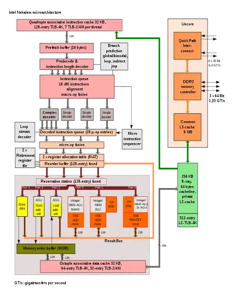
Capabilities of an AGU depend on a particular CPU and its architecture. Thus, some AGUs implement and expose more address-calculation operations, while some also include more advanced specialized instructions that can operate on multiple operands at a time.[2][3] Furthermore, some CPU architectures include multiple AGUs so more than one address-calculation operation can be executed simultaneously, bringing further performance improvements by capitalizing on the superscalar nature of advanced CPU designs. For example, Intel incorporates multiple AGUs into its Sandy Bridge and Haswell microarchitectures, which increase bandwidth of the CPU memory subsystem by allowing multiple memory-access instructions to be executed in parallel.[4][5][6]
See also
- Arithmetic logic unit (ALU) – a digital circuit that performs arithmetic and bitwise logical operations on integer binary numbers
- Floating-point unit (FPU) – the same as ALU but for floating-point numbers
- Load–store unit
- Bulldozer (microarchitecture) – another CPU microarchitecture that includes multiple AGUs, developed by AMD
- Register renaming – a technique that reuses CPU registers and avoids unnecessary serialization of program operations
- Reservation station – a CPU feature that allows results of various operations to be used while bypassing CPU registers
- Execution unit
References
- Cornelis Van Berkel; Patrick Meuwissen (January 12, 2006). "Address generation unit for a processor (US 2006010255 A1 patent application)". google.com. Retrieved December 8, 2014.
- "Chapter 4: Address Generation Unit (DSP56300 Family Manual)" (PDF). ecee.colorado.edu. September 16, 1999. Archived from the original (PDF) on March 29, 2018. Retrieved December 8, 2014.
- Darek Mihocka (December 27, 2000). "Pentium 4: Round 1 – Intel blows the lead". emulators.com. Retrieved December 8, 2014.
- David Kanter (September 25, 2010). "Intel's Sandy Bridge Microarchitecture: Memory Subsystem". realworldtech.com. Retrieved December 8, 2014.
- David Kanter (November 13, 2012). "Intel's Haswell CPU Microarchitecture: Haswell Memory Hierarchy". realworldtech.com. Retrieved December 8, 2014.
- Per Hammarlund (August 2013). "Fourth-Generation Intel Core Processor, codenamed Haswell" (PDF). hotchips.org. p. 25. Archived from the original (PDF) on July 5, 2016. Retrieved December 8, 2014.
External links
- Address generation unit in the Motorola DSP56K family, June 2003, Motorola
- Address generation unit in DSP applications, September 2013, by Andreas Ehliar
- Computer Science from the Bottom Up, Chapter 3. Computer Architecture, September 2013, by Ian Wienand