POWER1
The POWER1 is a multi-chip CPU developed and fabricated by IBM that implemented the POWER instruction set architecture (ISA). It was originally known as the RISC System/6000 CPU or, when in an abbreviated form, the RS/6000 CPU, before introduction of successors required the original name to be replaced with one that used the same naming scheme (POWERn) as its successors in order to differentiate it from the newer designs.
| General information | |
|---|---|
| Launched | 1990 |
| Designed by | IBM |
| Architecture and classification | |
| Instruction set | POWER ISA |
| History | |
| Successor(s) | POWER2 |
| POWER, PowerPC, and Power ISA architectures |
|---|
| NXP (formerly Freescale and Motorola) |
| IBM |
|
| IBM/Nintendo |
| Other |
| Related links |
| Cancelled in gray, historic in italic |
History
The POWER1 was introduced in 1990, with the introduction of the IBM RS/6000 POWERserver servers and POWERstation workstations, which featured the POWER1 clocked at 20, 25 or 30 MHz. The POWER1 received two upgrades, one in 1991, with the introduction of the POWER1+ and in 1992, with the introduction of POWER1++. These upgraded versions were clocked higher than the original POWER1, made possible by improved semiconductor processes. The POWER1+ was clocked slightly higher than the original POWER1, at frequencies of 25, 33 and 41 MHz, while the POWER1++ took the microarchitecture to its highest frequencies — 25, 33, 41.6, 45, 50 and 62.5 MHz. In September 1993, the POWER1 and its variants was succeeded by the POWER2 (known briefly as the "RIOS2"), an evolution of the POWER1 microarchitecture.
The direct derivatives of the POWER1 are the RISC Single Chip (RSC), feature-reduced single-chip variant for entry-level RS/6000 systems, and the RAD6000, a radiation-hardened variant of the RSC for space applications. An indirect derivative of the POWER1 is the PowerPC 601, a feature-reduced variant of the RSC intended for consumer applications.
The POWER1 is notable as it represented a number of firsts for IBM and computing in general. It was IBM's first RISC processor intended for high-end applications (the ROMP was considered a commercial failure and was not used in high-end workstations), it was the first to implement the then new POWER instruction set architecture and it was IBM's first successful RISC processor. For computing firsts, the POWER1 would be known for being the first CPU to implement some form of register renaming and out-of-order execution, a technique that improves the performance of superscalar processors but was previously reserved for mainframes.
The POWER1 was also the origin for the highly successful families of POWER, PowerPC and Power ISA processors that followed it, measuring in hundreds of different implementations.
The open source GCC compiler removed support for POWER1 (RIOS) and POWER2 (RIOS2) in the 4.5 release.[1]
Microarchitecture
The POWER1 is a 32-bit two-way superscalar CPU. It contains three major execution units, a fixed-point unit (FXU), a branch unit (BPU) and a floating point unit (FPU). Although the POWER1 is a 32-bit CPU with a 32-bit physical address, its virtual address is 52 bits long. The larger virtual address space was chosen because it was beneficial for the performance of applications, allowing each one to have a large 4 GB address range.
The POWER1 is a big-endian CPU that uses a Harvard style cache hierarchy with separate instruction and data caches. The instruction cache, referred to as the "I-cache" by IBM, is 8 KB in size and is two-way set associative with a line size of 64 bytes. The I-cache is located on the ICU chip. The data cache, referred to as the "D-cache" by IBM, is 32 KB in size for RIOS.9 configurations and 64 KB in size for RIOS-1 configurations. The D-cache is four-way set associative with a line size of 128 bytes. The D-cache employs a store-back scheme, where data that is to be stored is written to the cache instead of the memory in order to reduce the number of writes destined for the memory. The store-back scheme is used to prevent the CPU from monopolizing access to the memory.
Although the POWER1 was a high-end design, it was not capable of multiprocessing, and as such was disadvantaged, as the only way performance could be improved was by clocking the CPU higher, which was difficult to do with such a large multi-chip design. IBM used clustering to overcome this disadvantage in POWER1 systems, allowing them to effectively function as if they were multiprocessing systems, a concept proven by the popularity of SP1 supercomputers based on the POWER1. As the POWER1 was the basis of the POWER2 and P2SC microprocessors, the lack of multiprocessing was passed on to these later POWER processors. Multiprocessing was not supported until the introduction of the POWER3 in 1998.
Physical description


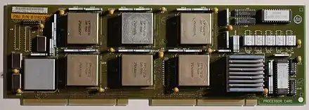
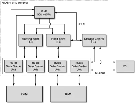
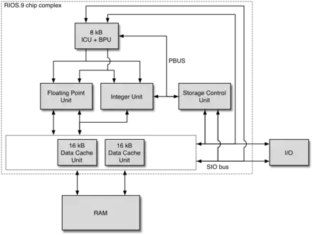
The POWER1 is a multi-chip CPU built from separate chips that are connected to each other by buses. The POWER1 consists of an instruction-cache unit (ICU), a fixed-point unit (FXU), a floating point unit (FPU), a number of data-cache units (DCU), a storage-control unit (SCU) and an I/O unit. Due to its modular design, IBM was able to create two configurations by simply varying the number of DCUs, RIOS-1 and a RIOS.9. The RIOS-1 configuration has four DCUs, the intended amount, and was clocked at up to 40 MHz, whereas the RIOS.9 CPU had two DCUs and was clocked at lower frequencies.
The chips are mounted on the “CPU planar”, a printed circuit board (PCB), using through-hole technology. Due to the large number of chips with wide buses, the PCB has eight planes for routing wires, four for power and ground and four for signals. There are two signal planes on each side of the board, while the four power and ground planes are in the center.
The chips that make up the POWER1 are fabricated in a 1.0 µm CMOS process with three layers of interconnect. The chips are packaged in ceramic pin grid array (CPGA) packages that can have up to 300 pins and dissipate a maximum of 4 W of heat each. The total number of transistors featured by the POWER1, assuming that it is a RIOS-1 configuration, is 6.9 million, with 2.04 million used for logic and 4.86 million used for memory. The die area of all the chips combined is 1,284 mm². The total number of signal pins is 1,464.
Instruction-cache unit (ICU)
The ICU contains the instruction cache, referred to as the "I-cache" by IBM and the branch processing unit (BPU). The BPU contains the program counter, the condition code register and a loop register. The ICU contains 0.75 million transistors with 0.2 million used for logic and 0.55 million used for SRAM. The ICU die measures approximately 160 mm² (12.7 × 12.7 mm).
The BPU was capable of dispatching multiple instructions to the fixed and floating point instructions queues while it was executing a program flow control instruction (up to four simultaneously and out of order). Speculative branches were also supported by using a prediction bit in the branch instructions, with the results discarded before being saved if the branch was not taken. The alternate instruction would be buffered and discarded if the branch was taken. Consequently, subroutine calls and interrupts are dealt with without incurring branch penalties.
The condition code register has eight field sets, with the first two reserved for fixed and floating point instructions and the seventh for vector instructions. The rest of the fields could be used by other instructions. The loop register is a counter for "decrement and branch on zero" loops with no branch penalty, a feature similar to those found in some DSPs such as the TMS320C30.
Fixed-point unit (FXU)
The FXU is responsible for decoding and executing all fixed-point instructions and floating-point load and store instructions. For execution, the FXU contains the POWER1's fixed-point register file, an arithmetic logic unit (ALU) for general instructions, and a dedicated fixed-point multiply and divide unit. It also contains instruction buffers that receive both fixed- and floating-point instructions from the ICU, passing on the floating-point instructions to the FPU, and a 128-entry two-way set-associative D-TLB for address translation. The FXU contains approximately 0.5 million transistors, with 0.25 million used for logic and 0.25 used for memory, on a die measuring approximately 160 mm².
Floating-point unit (FPU)
The POWER1's floating point unit executes floating-point instructions issue by the ICU. The FPU is pipelined and can execute single precision (32-bit) and double precision (64-bit) instructions. It is capable of performing multiply-add instructions, which contributed to the POWER1's high floating point performance. In most processors, a multiply and an add, which is common in technical and scientific floating-point code, cannot be executed in one cycle, as in the POWER1. Use of fused multiply–add also means that the data is only rounded once, improving the precision of the result slightly.
The floating-point register file is also located on the FPU chip. It contains 32 64-bit floating-point registers, six rename registers and two registers that are used by divide instructions.
Data-cache unit (DCU)
The POWER1 has a 64 KB data cache implemented through four identical data-cache units (DCU), each containing 16 KB of data cache. The cache and the buses that connect the DCU to the other chips are ECC protected. The DCUs also provide the interface to the memory. If two DCUs are present (RIOS.9 configuration), the memory bus is 64 bits wide, and if four DCUs are present (RIOS-1 configuration), the memory bus is 128 bits wide. The memory interface portion of the DCUs provide three features that improves the reliability and availability of the memory: memory scrubbing, ECC and bit steering. Each DCU contains approximately 1.125 million transistors, with 0.175 million used for logic and 0.95 million used for SRAM, on a die measuring approximately 130 mm² (11.3 × 11.3 mm).
Storage-control unit (SCU)
The POWER1 is controlled by the SCU chip. All communications between the ICU, FXU and DCU chips as well as the memory and I/O devices is arbitrated by the SCU. Although the DCUs provide the means to perform memory scrubbing, it is the SCU that controls the process. The SCU contains approximately 0.23 million transistors, all of them for logic, on a die measuring approximately 130 mm².
I/O unit
The POWER1's I/O interfaces are implemented by the I/O unit, which contains an I/O channel controller (IOCC) and two serial link adapters (SLAs). The IOCC implements the Micro Channel interface and controls both I/O and DMA transactions between the Micro Channel adapters and the system memory. The two SLAs each implement a serial fibre optic link, which are intended to connect RS/6000 systems together. The optical links were not supported at the time of the RS/6000's release. The I/O unit contains approximately 0.5 million transistors, with 0.3 million used for logic and 0.2 million used for memory, on a die measuring approximately 160 mm².
See also
- Instruction set architectures: IBM POWER Instruction Set Architecture, PowerPC, Power ISA
- Processors: RISC Single Chip, RAD6000, POWER2, POWER3, POWER4, POWER5, POWER6, POWER7, POWER8, POWER9, Power10
- Computer Systems: RS/6000, Scalable POWERparallel
- Related technology: PowerPC 601, RS64
References
- Great Microprocessors of the Past and Present (V 13.4.0)
- Montoye, R. K.; Hokenek, E.; Runyon, S. L. (January 1990). "Design of the IBM RISC System/6000 floating-point execution unit". IBM Journal of Research and Development. 34 (1): 59–70. doi:10.1147/rd.341.0059.
- Oehler, R. R.; Groves, R. D. (January 1990). "IBM RISC System/6000 processor architecture". IBM Journal of Research and Development. 34 (1): 23–36. doi:10.1147/rd.341.0023.
- Grohoski, G. F. (January 1990). "Machine organization of the IBM RISC System/6000 processor". IBM Journal of Research and Development. 34 (1): 37–58. doi:10.1147/rd.341.0037.
- Bakoglu, H. B.; Grohoski, G. F.; Montoye, R. K. (January 1990). "The IBM RISC System/6000 processor: Hardware overview". IBM Journal of Research and Development. 34 (1): 12–22. doi:10.1147/rd.341.0012.
Further reading
- Weiss, Shlomo; Smith, James Edward (1994). POWER and PowerPC. Morgan Kaufmann. ISBN 1558602798. — Relevant parts: Chapter 3 (how the POWER architecture is meant to be implemented), Chapters 4 and 5 (describes the POWER1).