Espresso (processor)
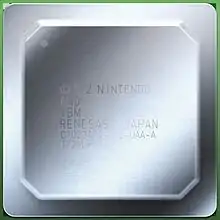
Espresso is the codename of the 32-bit central processing unit (CPU) used in Nintendos Wii U video game console. It was designed by IBM, and was produced using a 45 nm silicon-on-insulator process. The Espresso chip resides together with a GPU from AMD on an MCM manufactured by Renesas. It was revealed at E3 2011 in June 2011 and released in November 2012.
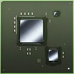
 An illustration of the Wii U MCM without heat spreader. The smaller chip, lower right, is the "Espresso" CPU made by IBM. The other chips are the "Latte" GPU (large chip, center) from AMD and an EEPROM chip (tiny chip, upper right) from Renesas. | |
| General information | |
|---|---|
| Launched | 2012 |
| Discontinued | January 31, 2017 |
| Marketed by | Nintendo |
| Designed by | IBM, Nintendo IRD, NTD |
| Common manufacturer(s) |
|
| Performance | |
| Max. CPU clock rate | 1.243 GHz |
| Cache | |
| L2 cache | 1× 2 MB, 2× 512 KB (on-die) |
| Last level cache | 3 |
| Architecture and classification | |
| Application | Embedded (Wii U) |
| Technology node | 45 nm |
| Microarchitecture | Not verified by Nintendo |
| Instruction set | PowerPC 1.1 |
| Instructions | 4 |
| Physical specifications | |
| Cores |
|
| GPU(s) | AMD Radeon-based "Latte" |
| History | |
| Predecessor(s) | Broadway |
| Successor(s) | Erista |
| POWER, PowerPC, and Power ISA architectures |
|---|
| NXP (formerly Freescale and Motorola) |
| IBM |
|
| IBM/Nintendo |
| Other |
| Related links |
| Cancelled in gray, historic in italic |
Design


IBM and Nintendo have revealed that the Espresso processor is a PowerPC-based microprocessor with three cores on a single chip to reduce power consumption and increase speed. The CPU and the graphics processor are placed on a single substrate as a multi-chip module (MCM) to reduce complexity, increase the communication speed between the chips, further reduce power consumption and reduce cost and space required. The two chips were assembled to the complete MCM by Renesas in Japan.[1] Espresso itself was manufactured by IBM in its 300 mm plant in East Fishkill, New York, using 45 nm SOI-technology[2] and embedded DRAM (eDRAM) for caches.
While unverified by Nintendo, hackers, teardowns, and unofficial informants have since revealed more information about the Espresso, such as its name,[3] size[4][5] and speed.[6][7] The microarchitecture seems to be quite similar to its predecessors the Broadway and Gekko, i.e. PowerPC 750 based, but enhanced with larger and faster caches and multiprocessor support.
Rumors that the Wii U CPU was derived from IBM's high-end POWER7 server processor proved false, as it would potentially increase the manufacturing and retail cost of the system, and require a larger form factor. Espresso shares some technology with POWER7, such as eDRAM and general instruction set similarities, but those are superficial similarities.[8][9][10][11][12]
Specifications
- Out-of-order execution PowerPC based cores
- 45 nanometer process technology
- IBM silicon on insulator (SOI) technology
- Backward compatible with the Broadway and Gekko processors
The following specifications have not been officially confirmed by either Nintendo or IBM. They have been obtained by reverse engineering by hacker Hector Martin, alias marcan.[13]
- Broadway-based core architecture[14]
- Three cores at 1.243125 GHz
- Symmetric multiprocessing with MESI/MERSI support[15]
- Each core can output up to 4 instructions per clock using superscalar parallelism.
- 32-bit integer unit
- 64-bit floating-point (or 2× 32-bit SIMD, often found under the denomination "paired singles")
- A total of 3 MB of Level 2 cache in an unusual configuration.[16]
- Core 0: 512 KB, core 1: 2 MB, core 2: 512 KB
- 4 stage pipeline [17]
- 7 stage pipeline - FP[17]
- 6 Execution Units per core (18 EUs total)[17]
- Die size: 4.74 mm × 5.85 mm = 27.73 mm2
References
- "Wii U : The Console : Changes in Television". Iwata Asks. Nintendo. Archived from the original on 2022-06-09.
- "NEW WII U™ ON SOI". Archived from the original on 2016-03-25.
- "World Exclusive: Wii U Final Specs". 11 September 2012.
- "Nintendo Wii U Teardown". AnandTech.
- "Nintendo Wii U Teardown". iFixit. 19 November 2012.
- "Wii U has 1.24GHz CPU, 550MHz graphics core". Eurogamer.net. 29 November 2012.
- "Wii U CPU, GPU Details Uncovered". 29 November 2012.
- "IBM puts Watson's brains in Nintendo Wii U".
- "IBM teases on Wii U CPU specs". Eurogamer.net. 8 June 2011.
- "Rumored Wii U Specs Raising Eyebrows... for the Wrong Reasons".
- "IBM reconfirms the Wii U/Watson connection". 27 August 2012.
- "IBM Confirms WII U Utilizes Power-Based CPU, Not Power 7". 25 September 2012.
- Joel Hruska (November 29, 2012). "Hackers Discover Wii U's Processor Design and Clock Speed". HotHardware. Retrieved January 21, 2014.
- Martín, Héctor [@marcan42] (2012-12-09). "@DFaker no, it's just a 750. PPC750 can issue 3/cycle and retire 2/cycle. @dampflokfreund yes, three Broadways and more cache" (Tweet). Archived from the original on 2013-10-05 – via Twitter.
- Martín, Héctor [@marcan42] (2013-11-23). "Hah! My Twitter arguing must be so sad that I just got this screenshot in my inbox (anon sender): marcansoft.com/transf/espresso_intro.png … @EyeOfCore" (Tweet). Archived from the original on 2013-12-03 – via Twitter. (links to PNG of a page from the IBM Espresso RISC Processor Developer's User Manual)
- Martín, Héctor [@marcan42] (2013-01-30). "@theevilmuppet L1 is the same, L2 is different (this is the claimed eDRAM). 512K/2M/512K L2 cache per core (core 1 has more cache)" (Tweet). Archived from the original on 2013-10-08 – via Twitter.
- "IBM PowerPC 750CL Microprocessor Revision Level DD2.x Datasheet" (PDF).