Gekko (processor)
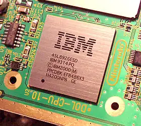
Gekko is a superscalar out-of-order 32-bit PowerPC microprocessor custom-made by IBM in 2000 for Nintendo to use as the CPU in their sixth generation game console, the GameCube, and later the Triforce Arcade Board.
 IBM Gekko processor | |
| General information | |
|---|---|
| Launched | 2000 |
| Discontinued | 2007 |
| Designed by | IBM and Nintendo |
| Common manufacturer(s) | |
| Performance | |
| Max. CPU clock rate | 486 MHz |
| Cache | |
| L1 cache | 32/32 KB |
| L2 cache | 256 KB |
| Architecture and classification | |
| Application | GameCube Triforce Arcade Board |
| Technology node | 180 nm |
| Microarchitecture | PowerPC G3 |
| Instruction set | PowerPC ISA 1.10 |
| Physical specifications | |
| Cores |
|
| Products, models, variants | |
| Variant(s) | |
| History | |
| Predecessor(s) | NEC VR4300 |
| Successor(s) | Broadway |

| POWER, PowerPC, and Power ISA architectures |
|---|
| NXP (formerly Freescale and Motorola) |
| IBM |
|
| IBM/Nintendo |
| Other |
| Related links |
| Cancelled in gray, historic in italic |
Development
Gekko's role in the game system was to facilitate game scripting, Artificial Intelligence, physics and collision detection, custom graphics lighting effects and geometry such as smooth transformations, and moving graphics data through the system.
The project was announced in 1999 when IBM and Nintendo agreed to a $1 billion dollar contract (IBM's largest ever single order)[1] for a CPU running at approximately 400 MHz. IBM chose to modify their existing PowerPC 750CXe processor to suit Nintendo's needs, such as tight and balanced operation alongside the "Flipper" graphics processor. The customization was to the bus architecture, DMA, compression and floating point unit which support a special set of SIMD instructions. The CPU made ground work for custom lighting and geometry effects and could burst compressed data directly to the GPU.
The Gekko is considered to be the direct ancestor to the Broadway processor, also designed and manufactured by IBM, that powers the Wii console.
Features
- Customized PowerPC 750CXe core
- Clockrate – 486 MHz
- Superscalar Out-of-order execution
- 4 stages long two-integer ALUs (IU1 and IU2) – 32 bit
- 7 stages long Floating Point Unit – 64-bit double-precision FPU, usable as 2 × 32-bit SIMD for 1.9 single-precision GFLOPS performance using the Multiply–accumulate operation. The SIMD is often found under the denomination "paired singles."
- Branch Prediction Unit (BPU)
- Load-Store Unit (LSU)
- System Register Unit (SRU)
- Memory Management Unit (MMU)
- Branch Target Instruction Cache (BTIC)
- SIMD Instructions – PowerPC750 + roughly 50 new SIMD instructions, geared toward 3D graphics
- Front-side Bus – 64-bit enhanced 60x bus to GPU/chipset at 162 MHz clock with 1.3 GB/s peak bandwidth
- On-chip Cache – 64 KB 8-way associative L1 cache (32/32 KB instruction/data). 256 KB on-die, 2-way associative L2 cache
- DMIPS – 1125 (dhrystone 2.1)
- 180 nm IBM six-layer, copper-wire process. 43 mm² die
- 1.8 V for logic and I/O. 4.9 W dissipation
- 27 × 27 mm PBGA package with 256 contacts
- 6.35 million logic transistors and 18.6 million transistors total
See also
- Broadway (microprocessor), the processor in the Wii
- MIPS R4300, the processor in the Nintendo 64
References
- "DataStream" (PDF). Edge. No. 79 (December 1999). 24 November 1999. p. 132.