UltraRAM
UltraRAM is a brand name and a storage device technology that is under development. The Physics and Engineering department of Lancaster University in collaboration with Department of Physics at Warwick published a paper[1] in the journal of advanced electronic materials suggesting an improvement in non volatile memory technology. It has been described as a memory storage technology that "combines the non-volatility of a data storage memory, like flash, with the speed, energy-efficiency, and endurance of a working memory, like DRAM" which means it could retain data like a hard drive.[2] While the Lancaster team performed some basic experiments to demonstrate the principles in action, UltraRAM remains mostly theoretical at the moment.[3] The Lancaster University researchers say that further work is ongoing to improve quality, fine-tune the fabrication process, and implement and scale UltraRAM devices.[4]

| Computer memory and data storage types |
|---|
| Volatile |
| Non-volatile |
History
In 2023 Quinas company formed to further develop Ultraram.[5]
Memory Concept
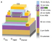
ULTRARAM is a charge-based memory where the logic state is determined by the presence or absence of electrons in an FG (Front Gate). The FG is electrically isolated from the control gate (CG) by Al2O3 dielectric, and from the underlying channel by the InAs/AlSb TBRT heterostructure. The presence of electrons in the FG (defining a logic 0 state) depletes carriers in the underlying n-type InAs channel, reducing its conductance. Thus, the charge state of the FG and, therefore, the logic state of the memory, is read nondestructively by measuring the current through the channel when a voltage is applied between the source (S) and drain (D) contacts. The final component of the memory is the InAs back-gate (BG), which allows voltages to be applied vertically across the gate stack for various operations.
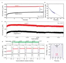
The novelty underpinning the memory is the TBRT (Triple Barrier Resonant Tunneling) structure, which, unlike single layer barriers, can be switched from a highly electrically resistive state to a highly conductive state by the application of just ±2.5 V. This is achieved by careful design of the thicknesses of the AlSb barriers and InAs QW (Quantum Well) layers. When the memory is in the retention state, i.e., when no voltage is applied to the device, the electron ground states in the TBRT QWs are misaligned with each other and are energetically well above the 300 K electron populations of the InAs FG and channel layers. Indeed, nonvolatility is strengthened by the QW ground states residing at an unusually high energy for a resonant-tunneling structure. This is due to a combination of the ultrathin QWs and the extraordinarily low electron effective mass in InAs. In this state, the TBRT provides a large barrier that prevents electron transfer into or out of the FG. However, the application of a suitable bias across the device tilts the conduction band such that the TBRT QW ground states align with occupied electron states in the channel (during the program operation) or the FG (during the erase operation). This allows electrons to move rapidly across the TBRT region in the intended direction by the inherently fast quantum-mechanical process of resonant tunneling. Due to the low voltages required and the low capacitance per unit area of the device compared to DRAM, ultralow logic state switching energies of 10−17 J are predicted for 20 nm feature size ULTRARAM memories, which is two and three orders of magnitude lower than DRAM and flash respectively. However, before this ultralow switching energy can be realized by fabricating nm-scale devices, the fundamental properties of μm-scale devices must first be understood and optimized. ULTRARAM prototype devices grown on GaAs substrates have previously exhibited experiment-limited, not device-limited, nonvolatile retention of 105 s and an endurance of 106 program-erase cycles.[1]
Operations

A charged FG is defined as logic '0', and the absence of charge as logic '1'. Program and erase cycles, to charge and discharge the FG respectively, use voltage pulses of ≤±2.55 V on the CG.
InAs channel transistors with submicrometer feature sizes and a subthreshold swing of <100 mV/dec have previously been demonstrated.[6] Consequently, due to the threshold voltage window of 350 mV in the devices designed by the Lancaster team, one can expect the 0/1 current contrast of ULTRARAM to improve to three decades with the implementation of a normally-off channel. Such an improvement of the 0/1 contrast through careful modification of the channel will allow memory arrays to be built with a novel high-density RAM architecture.[1]
Significance
The ULTRARAM on silicon devices actually outperform previous incarnations of the technology on GaAs compound semiconductor wafers, demonstrating (extrapolated) data storage times of at least 1000 years, fast switching speed (for device size) and program-erase cycling endurance of at least 10 million, which is one hundred to one thousand times better than flash. Professor Manus Hayne of the Department of Physics at Lancaster, who leads the work said, "ULTRARAM on silicon is a huge advance for our research, overcoming very significant materials challenges of large crystalline lattice mismatch, the change from elemental to compound semiconductor and differences in thermal contraction."[2]
Accolades
On August 11, 2023, it won the "Most Innovative Flash Memory Startup" award at the 17th Flash Memory Summit (FMS 2023). [7]
References
- Hodgson, Peter D.; Lane, Dominic; Carrington, Peter J.; Delli, Evangelia; Beanland, Richard; Hayne, Manus (2022-01-05). "ULTRARAM: A Low-Energy, High-Endurance, Compound-Semiconductor Memory on Silicon". Advanced Electronic Materials. 8 (4): 2101103. doi:10.1002/aelm.202101103. ISSN 2199-160X. S2CID 248070399.
- "Mass production of revolutionary computer memory moves closer with ULTRARAM on silicon wafers for the first time". ScienceDaily. Retrieved 2022-04-08.
- "'UltraRAM' breakthrough could merge storage and RAM into one component". PCWorld. Retrieved 2022-04-08.
- Mark Tyson (2022-01-10). "UltraRAM Breakthrough Brings New Memory and Storage Tech to Silicon". Tom's Hardware. Retrieved 2022-04-08.
- published, Mark Tyson (2023-09-26). "UltraRAM Demos Prototype Chip, Secures Funding to Validate Commercial Potential". Tom's Hardware. Retrieved 2023-09-26.
- Chang, S. W.; Li, Xu; Oxland, R.; Wang, S. W.; Wang, C. H.; Contreras-Guerrero, R.; Bhuwalka, K. K.; Doornbos, G.; Vasen, T.; Holland, M. C.; Vellianitis, G. (30 January 2014). "InAs N-MOSFETs with record performance of Ion = 600 μA/μm at Ioff = 100 nA/μm (Vd = 0.5 V)". 2013 IEEE International Electron Devices Meeting. pp. 16.1.1–16.1.4. doi:10.1109/IEDM.2013.6724639. ISBN 978-1-4799-2306-9. S2CID 10847457.
- "Flash Memory Summit Announces 2023 Best of Show Award Winners". kalkinemedia.com. 2023-08-12. Retrieved 2023-09-28.
External links
- Nasser, Hussein (19 Jan 2022). "Is ULTRARAM a game changer?". YouTube.
- Promotion video: https://www.youtube.com/watch?v=iz-sYyfojw4