Bubble memory
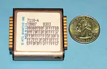
Bubble memory is a type of non-volatile computer memory that uses a thin film of a magnetic material to hold small magnetized areas, known as bubbles or domains, each storing one bit of data. The material is arranged to form a series of parallel tracks that the bubbles can move along under the action of an external magnetic field. The bubbles are read by moving them to the edge of the material, where they can be read by a conventional magnetic pickup, and then rewritten on the far edge to keep the memory cycling through the material. In operation, bubble memories are similar to delay-line memory systems.
| Computer memory and data storage types |
|---|
| Volatile |
| Non-volatile |
Bubble memory started out as a promising technology in the 1970s, offering memory density of an order similar to hard drives, but performance more comparable to core memory, while lacking any moving parts. This led many to consider it a contender for a "universal memory" that could be used for all storage needs. The introduction of dramatically faster semiconductor memory chips pushed bubble into the slow end of the scale, and equally dramatic improvements in hard-drive capacity made it uncompetitive in price terms.[1] Bubble memory was used for some time in the 1970s and 1980s where its non-moving nature was desirable for maintenance or shock-proofing reasons. The introduction of flash storage and similar technologies rendered even this niche uncompetitive, and bubble disappeared entirely by the late 1980s.
History
Precursors
Bubble memory is largely the brainchild of a single person, Andrew Bobeck. Bobeck had worked on many kinds of magnetics-related projects through the 1960s, and two of his projects put him in a particularly good position for the development of bubble memory. The first was the development of the first magnetic-core memory system driven by a transistor-based controller, and the second was the development of twistor memory.
Twistor is essentially a version of core memory that replaces the "cores" with a piece of magnetic tape. The main advantage of twistor is its ability to be assembled by automated machines, as opposed to core, which was almost entirely manual. AT&T had great hopes for twistor, believing that it would greatly reduce the cost of computer memory and put them in an industry leading position. Instead, DRAM memories came onto the market in the early 1970s and rapidly replaced all previous random-access memory systems. Twistor ended up being used only in a few applications, many of them AT&T's own computers.
One interesting side effect of the twistor concept was noticed in production: under certain conditions, passing a current through one of the electrical wires running inside the tape would cause the magnetic fields on the tape to move in the direction of the current. If used properly, it allowed the stored bits to be pushed down the tape and pop off the end, forming a type of delay-line memory, but one where the propagation of the fields was under computer control, as opposed to automatically advancing at a set rate defined by the materials used. However, such a system had few advantages over twistor, especially as it did not allow random access.
Development
In 1967, Bobeck joined a team at Bell Labs and started work on improving twistor. The memory density of twistor was a function of the size of the wires; the length of any one wire determined how many bits it held, and many such wires were laid side-by-side to produce a larger memory system.
Conventional magnetic materials, like the magnetic tape used in twistor, allowed the magnetic signal to be placed at any location and to move in any direction. Paul Charles Michaelis working with permalloy magnetic thin films discovered that it was possible to move magnetic signals in orthogonal directions within the film. This seminal work led to a patent application.[2] The memory device and method of propagation were described in a paper presented at the 13th Annual Conference on Magnetism and Magnetic Materials, Boston, Massachusetts, 15 September 1967. The device used anisotropic thin magnetic films that required different magnetic pulse combinations for orthogonal propagation directions. The propagation velocity was also dependent on the hard and easy magnetic axes. This difference suggested that an isotropic magnetic medium would be desirable.
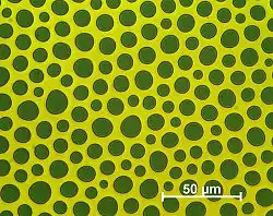
This led to the possibility of making a memory system similar to the moving-domain twistor concept, but using a single block of magnetic material instead of many twistor wires. Starting work extending this concept using orthoferrite, Bobeck noticed an additional interesting effect. With the magnetic tape materials used in twistor, the data had to be stored on relatively large patches known as domains. Attempts to magnetize smaller areas would fail. With orthoferrite, if the patch was written and then a magnetic field was applied to the entire material, the patch would shrink down into a tiny circle, which he called a bubble. These bubbles were much smaller than the domains of normal media like tape, which suggested that very high area densities were possible.
Five significant discoveries took place at Bell Labs:
- The controlled two-dimensional motion of single wall domains in permalloy films
- The application of orthoferrites
- The discovery of the stable cylindrical domain
- The invention of the field access mode of operation
- The discovery of growth-induced uniaxial anisotropy in the garnet system and the realization that garnets would be a practical material
The bubble system cannot be described by any single invention, but in terms of the above discoveries. Andy Bobeck was the sole discoverer of (4) and (5) and co-discoverer of (2) and (3); (1) was performed by P. Michaelis in P. Bonyhard's group. At one point, over 60 scientists were working on the project at Bell Labs, many of whom have earned recognition in this field. For instance, in September 1974, H.E.D. Scovil, P.C. Michaelis and Bobeck were awarded the IEEE Morris N. Liebmann Memorial Award by the IEEE with the following citation: For the concept and development of single-walled magnetic domains (magnetic bubbles), and for recognition of their importance to memory technology.
It took some time to find the perfect material, but it was discovered that some garnets had the correct properties. Bubbles would easily form in the material and could be pushed along it fairly easily. The next problem was to make them move to the proper location where they could be read back out: twistor was a wire and there was only one place to go, but in a 2D sheet things would not be so easy. Unlike the original experiments, the garnet did not constrain the bubbles to move only in one direction, but its bubble properties were too advantageous to ignore.
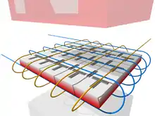
The solution was to imprint a pattern of tiny magnetic bars onto the surface of the garnet, called propagation elements. When a small magnetic field was applied, they would become magnetized, and the bubbles would "stick" to one end. By then reversing the field they would be attracted to the far end, moving down the surface. Another reversal would pop them off the end of the bar to the next bar in the line, and so on, controlling or guiding the direction of travel of the bubbles. T bars/guides, shaped like the letters, were used in early bubble memory designs, but were later replaced by other shapes such as asymmetrical chevrons.[3] In practice the magnetic field rotates and is provided by a pair of coils, that produce a rotating magnetic field in the X and Z axes, it is this rotating magnetic field that moves the bubbles in the memory.
Amorphous magnetic films were also considered as they had greater potential for improvement of bubble memories vs garnet magnetic films, however the existing experience with garnet films meant that they did not gain a foothold. Garnet films have the same or better magnetic properties than orthoferrite films which were considered less promising by comparison. Garnet materials (as films on top of a substrate) could allow for higher propagation speeds of the bubbles (bubble speed) than orthoferrites. Hard bubbles are slower and more erratic than normal bubbles, a problem that is often overcome by ion-implantation of the garnet magnetic film with neon,[4] and can also be done by coating the garnet magnetic film with permalloy.[5]
A memory device is formed by lining up tiny electromagnets at one end with detectors at the other end. Bubbles written in would be slowly pushed to the other, forming a sheet of twistors lined up beside each other. Attaching the output from the detector back to the electromagnets turns the sheet into a series of loops, which can hold the information as long as needed.[3]
Bubble memory is a non-volatile memory. Even when power was removed, the bubbles remained, just as the patterns do on the surface of a disk drive. Better yet, bubble memory devices needed no moving parts: the field that pushed the bubbles along the surface was generated electrically, whereas media like tape and disk drives required mechanical movement. Finally, because of the small size of the bubbles, the density was in theory much higher than existing magnetic storage devices. The only downside was performance; the bubbles had to cycle to the far end of the sheet before they could be read.
A bubble memory device consists of a case, that houses a PCB with connections to one or more bubble memory chips, which may be translucent. The area around the chips on the PCB is surrounded by two windings made of copper wire or other electrically conductive material, that mostly wrap the area, leaving some space for the PCB to pass through the windings and connect to the chips. The windings are wound in directions opposite to each other, for example one winding has wires oriented along the X axis and the other winding has wires along the Z axis. The windings, in turn, are surrounded by two permanent magnets, one below and another above the windings. This forms an assembly that is housed inside the case which acts as a magnetic shield and forms a magnetic return path for the magnetic field from the magnets. The permanent magnets are critical; they create a static (DC, direct current) magnetic field, used as a bias field that enables the contents of the memory to be retained, in other words they allow bubble memories to be non-volatile. If the magnets are removed, all bubbles will disappear and thus all contents will be deleted. The windings create a rotating magnetic field parallel to the orientation of the bubble memory, at around 100 to 200 khz. This will move or drive the bubbles in the magnetic film in a somewhat circular fashion, guided or restrained by the propagation elements. For example, the rotating magnetic field can force the bubbles to constantly circulate around loops, which may be elongated and are defined by the locations of the guiding elements.[3][6]
To allow the bubbles to move around the bubble chips and to guide them through the chip, the chips have some sort of pattern made of ferromagnetic metal that can include for examplie asymmetrical chevrons.[3] For example, the bubbles can move around the edges of the chevrons. The patterns can be called propagation elements as they allow the bubbles to move or propagate across it. They define pathways for the bubbles to be stored and retrieved for reading and the rotating magnetic field moves the bubbles along these paths. For bubble memory, a material like Gadolinium Gallium Garnet is used as the substrate in the chips.[3] On top of the substrate is a magnetic film (bubble host or bubble film/layer)[5][4] such as a Gadolinium-containing garnet[5] or more often, single crystal substituted yttrium iron garnet[4] which holds the magnetic bubbles, that is grown epitaxially with liquid-phase epitaxy with lead oxide flux as the liquid with yttrium oxide and other oxides, and then the film is doped with ion-implantation of one or several elements, to reduce undesirable characteristics.[5][3] The epitaxy process would be carried out with a platinum crucible and wafer holder.[4] The chevrons and other parts are built on top of the film.[3] The propagation elements, including the chevrons, can be made of a material such as Nickel-Iron permalloy. The materials in bubble memories are chosen mainly for their magnetic properties.[3] Gadolinium Gallium Garnet is used as a substrate because it can support the epitaxial growth of magnetic garnet films, and is nonmagnetic,[4] although some bubble memories used Nickel-Cobalt substrates instead.
The use of propagation elements formed by ion implantation instead of permalloy, was proposed to increase the capacity of bubble memory to 16 Mbit/cm2.[4]
Commercialization
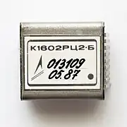
Bobeck's team soon had 1 cm (0.39 in) square memories that stored 4,096 bits, the same as a then-standard plane of core memory. This sparked considerable interest in the industry. Not only could bubble memories replace core but it seemed that they could replace tapes and disks as well. In fact, it seemed that bubble memory would soon be the only form of memory used in the vast majority of applications, with the high-performance market being the only one they could not serve.
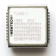
The technology was included in experimental devices from Bell Labs in 1974.[7] By the mid-1970s, practically every large electronics company had teams working on bubble memory.[8] Texas Instruments introduced the first commercial product that incorporated bubble memory in 1977, and introduced the first commercially available bubble memory, the TIB 0103 with 92 kilobit capacity.[9][10][11] By the late 1970s several products were on the market, and Intel released their own 1-megabit version, the 7110, in 1979.[12][13][14] By the early 1980s, however, bubble memory technology became a dead end with the introduction of hard disk systems offering higher storage densities, higher access speeds, and lower costs. In 1981 major companies working on the technology closed their bubble memory operations,[15] notably Rockwell, National Semiconductor, Texas Instruments and Plessey, leaving a "big five" group of companies still pursuing "second-generation bubble" by 1984: Intel, Motorola, Hitachi, Sagem and Fujitsu.[16] 4-megabit bubble memories such as the Intel 7114, were introduced in 1983[17][18][19] and 16-megabit bubble memory was developed.[20][21]
Bubble memory found uses in niche markets through the 1980s in systems needing to avoid the higher rates of mechanical failures of disk drives, and in systems operating in high vibration or harsh environments. This application became obsolete too with the development of flash storage, which also brought performance, density, and cost benefits.
One application was Konami's Bubble System arcade video game system, introduced in 1984. It featured interchangeable bubble memory cartridges on a 68000-based board. The Bubble System required a "warm-up" time of about 85 seconds (prompted by a timer on the screen when switched on) before the game was loaded, as bubble memory needs to be heated to around 30 to 40 °C (86 to 104 °F) to operate properly. Fujitsu used bubble memory on their FM-8 in 1981 and Sharp used it in their PC 5000 series, a laptop-like portable computer from 1983. Nicolet used bubble memory modules for saving waveforms in their Model 3091 oscilloscope, as did HP who offered a $1595 bubble memory option that extended the memory on their model 3561A digital signal analyzer. GRiD Systems Corporation used it in their early laptops. TIE communication used it in the early development of digital phone systems in order to lower their MTBF rates and produce a non-volatile telephone system's central processor.[22] Bubble memory was also used on the Quantel Mirage DVM8000/1 VFX system.
To store the bubbles, the propagation elements are in pairs and side to side, and are arranged in rows called loops to store the bubbles, thus they are storage loops since the bubbles that are stored in a loop will constantly circulate around it, forced by the rotating magnetic field that can also move the bubbles elsewhere. Bubble memories have extra spare loops to allow for increased yield during manufacturing as they replace defective loops. The list of defective loops is programmed onto the memory, on a special, separate loop called a boot loop, and it is also often printed on the label of the memory. A bubble memory controller will read the boot loop every time a bubble memory system is powered on, during initialization the controller will put the boot loop data in a boot loop register. Writing into a bubble memory is done by a formatter within the memory controller and signals from bits read in the bubble memory are amplified by the sense amplifier of the controller and they will reference the boot loop register to avoid overwriting, or further reading of the data in the boot loop.[3]
The bubbles are created (the memory is written) with a seed bubble that is constantly split or cut by a hairpin-shaped piece of electrically conductive wire (such as aluminum-copper alloy) using a current strong enough to locally overcome and reverse the magnetic bias field generated by the magnets, thus the hairpin-shaped piece of wire acts as a small electromagnet. The seed bubble regains its original size quickly after cutting. The seed bubble circulates under a circular permalloy patch which keeps it from moving elsewhere. After generation, the bubbles then circulate into an "input track" and then into a storage loop. Old bubbles would be moved out of the loop into an "output track" for destruction later. The space left behind by the old bubbles would then be available for new ones.[3] If the seed bubble is ever lost, a new one can be nucleated via special signals sent to the bubble memory and a current 2 to 4 times higher than necessary for cutting of bubbles from the seed bubble.[4]
The bubbles in a storage loop (and empty spaces for bubbles) constantly circulate around it. To read a bubble, it would be "replicated" by moving it to a larger propagation element to stretch the bubble, then it would be passed under a hairpin-shaped conductor to cut it into two with a current pulse which lasts 1/4 of a hertz and is shaped as a spike waveform with a long trailing edge, this would split the bubble in two, one of which would continue circulating in the storage loop, keeping the bubble and thus data safe in case of power failure. The other bubble would be moved to an output track to move it to a detector which is a magnetoresistive bridge, made of a column of interconnected permalloy chevrons where the chevrons are one behind the other, and before it there are similar columns of chevrons that are not interconnected. These stretch the bubbles to generate a larger output at the detector. The detector has a constant electric current, and when bubbles pass under it, they change slightly the electrical resistance and thus current in the detector, and the movement of the bubbles creates a voltage in the order of millivolts, and this is read as either a 1 or a 0. Because the bubble must be moved to a specific area to be read, there are latency constraints. After the detector the bubbles are run into a guard rail to destroy them. A 1 is represented by a bubble, and a 0 is represented by the absence of a bubble.[3]
The gadolinium gallium garnet wafers used as substrates for the bubble chips, were 3 inches in diameter and cost $100 each in 1982 as their production required the use of iridium crucibles.[4]
Further applications
In 2007, the idea of using microfluidic bubbles as logic (rather than memory) was proposed by MIT researchers. The bubble logic would use nanotechnology and has been demonstrated to have access times of 7 ms, which is faster than the 10 ms access times that present hard drives have, though it is slower than the access time of traditional RAM and of traditional logic circuits, making the proposal not commercially practical at present.[23]
IBM's 2008 work on racetrack memory is essentially a 1-dimensional version of bubble, bearing an even closer relationship to the original serial twistor concept.[24]
See also
- Gadolinium gallium garnet, used in many bubble memories as a substrate
References
- "Bubble Memory". 10 Technologies that were Supposed to Blow Up but Never Did. Complex. 2012-09-25. Archived from the original on 2012-10-08. Retrieved 2012-10-03.
- US patent 3,454,939, issued 1969-07-08
- Intel Memory Components Handbook. 1984.
- Rose, DONALD K.; Silverman, PETER J.; Washburn, HUDSON A. (1982-01-01), Einspruch, Norman G. (ed.), "Chapter 4 - Technology and Manufacturing of High-Density Magnetic-Bubble Memories", VLSI Electronics Microstructure Science, Elsevier, vol. 4, pp. 147–181, doi:10.1016/b978-0-12-234104-5.50010-x, retrieved 2023-09-07
- FOREIGN AND DOMESTIC ACCOMPLISHMENTS IN MAGNETIC BUBBLE DEVICE TECHNOLOGY. National Bureau of Standards. 1977. https://nvlpubs.nist.gov/nistpubs/Legacy/SP/nbsspecialpublication500-1.pdf
- Intel magnetics. 1 mega bit Bubble Memory Design Handbook. 1979.
- Stacy V. Jones (Feb 2, 1974). "Computer-Memory Aid Devised". New York Times. New York, N.Y. p. 37. ISSN 0362-4331. Archived from the original on 2018-01-12.
- Victor K. McElheny (Feb 16, 1977). "Technology: A Test for Magnetic Bubble Memories". New York Times. New York, N.Y. p. 77. ISSN 0362-4331. Archived from the original on 2018-01-11.
Among manufacturers of magnetic bubble units, besides Bell Labs and I.B.M., are Texas Instruments, the Honeywell Inc. process control division in Phoenix, and Rockwell International...
- "Canadian Electronics Engineering". Maclean-Hunter. March 3, 1978 – via Google Books.
- "Scientific American". Scientific American, Incorporated. March 3, 1977 – via Google Books.
- "Texas Instruments Introduces Portable Computer Terminal: Model Said to Be First With Mass Memory and Using Bubble Memory Device". Wall Street Journal. New York, N.Y.: Dow Jones & Company Inc. Apr 18, 1977. p. 13. ISSN 0099-9660.
- Enterprise, I. D. G. (May 7, 1979). "Computerworld". IDG Enterprise – via Google Books.
- Inc, InfoWorld Media Group (July 12, 1982). "InfoWorld". InfoWorld Media Group, Inc. – via Google Books.
{{cite web}}:|last=has generic name (help) - Inc, InfoWorld Media Group (May 9, 1979). "InfoWorld". InfoWorld Media Group, Inc. – via Google Books.
{{cite web}}:|last=has generic name (help) - Banks, Howard (September 20, 1981). "The Computer Bubble That Burst". New York Times. Archived from the original on 24 May 2015. Retrieved 17 October 2013.
- Reece, Charles (October 1984). "Bubble memory in data processing". Data Processing. pp. 26–28. Retrieved 2 March 2023.
- Computer Design. Computer Design Publishing Corporation. 1983.
- Electronics. McGraw-Hill Publishing Company. 1983.
- New Bubble-Memory Packaging Cuts Board Space And Manufacturing Costs. Intel AR-271.
- "Electronic Products Magazine". United Technical Publications. March 3, 1986 – via Google Books.
- "Journal of Electronic Engineering: JEE". Dempa Publications, Incorporated. March 3, 1985 – via Google Books.
- GRiD Compass 1101 computer Archived 2008-09-16 at the Wayback Machine, oldcomputers.net
- Prakash, Manu; Gershenfeld, Neil (9 February 2007). "Microfluidic Bubble Logic". Science. 315 (5813): 832–5. Bibcode:2007Sci...315..832P. doi:10.1126/science.1136907. JSTOR 20038959. PMID 17289994. S2CID 5882836.
- Parkin (11 April 2008). "Magnetic Domain-Wall Racetrack Memory". Science. 320 (5873): 190–4. Bibcode:2008Sci...320..190P. doi:10.1126/science.1145799. PMID 18403702. S2CID 19285283.
External links
- Great Microprocessors of the Past and Present. Appendix F: Memory Types: Web site by John Bayko
- The Arcade Flyer Archive: Konami Bubble System Flyer
- Bubbles: the better memory
- Whatever Happened to Bubble Memory?
- Magnetic Bubble Memories - Web site by George S. Almasi
- Novel Non-magnetic Bubble Memory
- Structure of a bubble memory
- An exploded view and photo of a dissasembled bubble memory, showing PCBs with memory bubble chips
- A file operating system ported to a modern bubble board