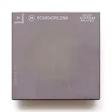
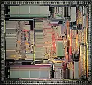
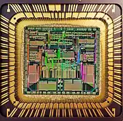
Motorola 68040
The Motorola 68040 ("sixty-eight-oh-forty") is a 32-bit microprocessor in the Motorola 68000 series, released in 1990. It is the successor to the 68030 and is followed by the 68060, skipping the 68050. In keeping with general Motorola naming, the 68040 is often referred to as simply the '040 (pronounced oh-four-oh or oh-forty).
| General information | |
|---|---|
| Launched | 1990 |
| Designed by | Motorola |
| Performance | |
| Max. CPU clock rate | 25 MHz to 40 MHz |
| Data width | 32 bits |
| Address width | 32 bits |
| Cache | |
| L1 cache | 4096 bytes each for instruction and data with independent MMU and TLB[1] |
| Architecture and classification | |
| Instruction set | Motorola 68000 series |
| Physical specifications | |
| Transistors |
|
| Package(s) | |
| Products, models, variants | |
| Variant(s) |
|
| History | |
| Predecessor(s) | Motorola 68030 |
| Successor(s) | Motorola 68060 |


The 68040 was the first 680x0 family member with an on-chip Floating-Point Unit (FPU). It thus included all of the functionality that previously required external chips, namely the FPU and Memory Management Unit (MMU), which was added in the 68030. It also had split instruction and data caches of 4 kilobytes each. It was fully pipelined, with six stages.
Versions of the 68040 were created for specific market segments, including the 68LC040, which removed the FPU, and the 68EC040, which removed both the FPU and MMU. Motorola had intended the EC variant for embedded use, but embedded processors during the 68040's time did not need the power of the 68040, so EC variants of the 68020 and 68030 continued to be common in designs.
Motorola produced several speed grades. The 16 MHz and 20 MHz parts were never qualified (XC designation) and used as prototyping samples. 25 MHz and 33 MHz grades featured across the whole line, but until around 2000 the 40 MHz grade was only for the "full" 68040. A planned 50 MHz grade was canceled after it exceeded the thermal design envelope.
Usage
In Apple Macintosh computers, the 68040 was introduced in the Macintosh Quadra, which was named for the chip. The fastest 68040 processor was clocked at 40 MHz and it was used only in the Quadra 840AV. The more expensive models in the (short-lived) Macintosh Centris line also used the 68040, while the cheaper Quadra, Centris and Macintosh Performa used the 68LC040. The 68040 was also used in other personal computers, such as the Amiga 4000 and Amiga 4000T, as well as a number of workstations, Alpha Microsystems servers, the HP 9000/400 series, NCR Corporation's TOWER 32/750, 32/825 and 32/850,[2] Apollo Computer's DN5500,[3] and later versions of the NeXT computer.
The 68040 processor is used in the flight management computers (FMC) aboard many Boeing 737 aircraft, including all Next Generation and MAX models.[4]
Design
The 68040 ran into the transistor budget limit early in design. While the MMU did not take many transistors—indeed, having it on the same die as the CPU actually saved on transistors—the FPU certainly did. Motorola's 68882 external FPU was known as a very high performance unit and Motorola did not wish to risk integrators using the "LC" version with a 68882 instead of the more profitable full "RC" unit. (For information on Motorola's multiprocessing model with the 680x0 series, see Motorola 68020.) The FPU in the 68040 was thus made incapable of IEEE transcendental functions, which had been supported by both the 68881 and 68882 and were used by the popular fractal generating software of the time and little else. The Motorola floating point support package (FPSP) emulated these instructions in software under interrupt. As this was an exception handler, heavy use of the transcendental functions caused severe performance penalties.
Heat was always a problem throughout the 68040's life. While it delivered over four times the per-clock performance of the 68020 and 68030, the chip's complexity and power requirements came from a large die and large caches. This affected the scaling of the processor and it was never able to run with a clock rate exceeding 40 MHz. A 50 MHz variant was planned, but canceled. Overclocking enthusiasts reported success reaching 50 MHz using a 100 MHz oscillator instead of an 80 MHz part and the then novel technique of adding oversized heat sinks with fans.
The 68040 offered the same features as the Intel 80486, but on a clock-for-clock basis could significantly outperform the Intel chip in integer and floating point instructions.[5][6]
Variants
68EC040
The 68EC040 is a version of the Motorola 68040 microprocessor, intended for embedded controllers (EC). It differs from the 68040 in that it has neither an FPU nor an MMU. This makes it less expensive and it draws less power. The 68EC040 was used in Cisco switch Supervisor Engine I that is the heart of models 2900, 2948G, 2980G, 4000, 4500, 5000, 5500, 6000, 6500 and 7600.
68LC040

The 68LC040 is a low cost version of the Motorola 68040 microprocessor with no FPU. This makes it less expensive and it draws less power. Although the CPU now fits into a feature chart more like the Motorola 68030, it continues to include the 68040's caches and pipeline and is thus significantly faster than the 68030.
Some mask revisions of the 68LC040 contained a bug that prevents the chip from operating correctly when a software FPU emulator is used. According to Motorola's errata,[7] any chip with a mask set 2E71M or later does not contain the bug. This new mask was introduced in mid-1995 and converted the 68LC040 chip to MC status.[8]
The buggy revisions are typically found in 68LC040-based Apple Macintosh computers. Chips with mask set 2E23G (as used in the LC 475) have been confirmed to be faulty. The fault relates to pending writes being lost when the F-line exception is triggered.[9] The 68040 cannot update its microcode in the manner of modern x86 chips. This means that the only way to use software that requires floating-point functionality is to replace the buggy 68LC040 with a later revision, or a full 68040.
Technical data
| CPU clock rate | 25, 33, 40 MHz |
| Production process | static CMOS 0.8 μm, 0.65 μm, Freescale 0.57 μm |
| Chip carrier | 179 ceramic PGA and 184 QFP |
| Address bus | 32 bit |
| Data bus | 32 bit |
| Instruction set | CISC |
| Transistors | ~1,200,000 |
ATC = Address Translation Cache
References
- "MC68040 Product Summary Page". Archived from the original on 14 January 2012.
- Fitzgerald, Michael (6 May 1991). "NCR promises Tower line lives". Computerworld. Retrieved 31 March 2023.
- Tim Hunkler (July 1996). "Survival Guide for Apollo Workstations". Retrieved 13 October 2022.
- Brady, Chris. "The Boeing 737 Flight Management Computer". The Boeing 737 Technical Site. Retrieved 24 June 2022.
- "CISC: The Intel 80486 vs. The Motorola MC68040". July 1992. Retrieved 20 May 2013.
- "68040 Microprocessor". Archived from the original on 16 February 2012.
- "Documentation Clarification for MC68040". Freescale. Archived from the original on 14 March 2012. Retrieved 20 May 2013.
- "E71M and E42K MC-Qualified Mask Sets". Freescale. Archived from the original on 2 March 2012. Retrieved 24 July 2012.
- "NetBSD Problem Report #13078: Mac 68LC040 problem". Gnats.netbsd.org. Retrieved 24 July 2012.
Further reading
- Savard, John J. G. (2018) [2007]. "The Decimal Floating-Point Standard". quadibloc. Other Recent Decimal Floating-Point Formats. Archived from the original on 3 July 2018. Retrieved 16 July 2018.