Heterostructure barrier varactor
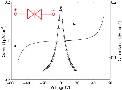
The heterostructure barrier varactor (HBV) is a semiconductor device which shows a variable capacitance with voltage bias, similar to a varactor diode. Unlike a diode, it has an anti-symmetric current-voltage relationship and a symmetric capacitance-voltage relationship, as shown in the graph to the right. The device was invented by Erik Kollberg together with Anders Rydberg in 1989[1] at Chalmers University of Technology.

The inset of the figure shows the circuit schematic symbol of the HBV. From the symbol, one can conclude that the HBV consists of two, back to back, anti-serially connected rectifying diodes (such as Schottky diodes for instance). The gap in the middle of the diode symbol represents the inherent capacitance of the device. The electrical characteristics of the HBV are realized by separating two layers of a semiconductor material (A) with a layer of another semiconductor material (B). The band-gap of material (B) should be larger than for material (A). This results in a barrier for the carriers trying to travel through the layers (A)-(B)-(A). The (A) layers are usually n-doped which means that electrons are the majority carriers of this device. At different bias voltages the carriers are redistributed and the distance between the carriers on each side of the barrier (B) is different. As a consequence the HBV has electrical properties resembling the parallel plate capacitor with a voltage dependent plate distance d.
The main application for the HBV diode is to generate extremely high frequency signals from lower frequency input. This type of frequency multiplication is demonstrated as triplers (3× multiplication) at 100 GHz[2] through 282 GHz[3] and up to 450 GHz,[4] and also as quintuplers (5× multiplication) at 175 GHz.[5]
The frequency multiplication is made possible by the highly nonlinear voltage dependence of the capacitance C(V). By feeding the HBV a signal of low frequency f1, higher harmonics f3=3f1 (tripler), f5=5f1 (quintupler), ... will be generated. Only odd harmonics are generated, since even harmonics are cancelled due to the symmetric nature of the nonlinearity. Also, using this inherent symmetry of the device, it can operate without DC-biasing. This is an advantage compared to the Schottky diode which has to be biased.
Signals generated at these frequencies (100 GHz – 3 THz) have applications in diverse areas such as radioastronomy, security imaging, biological and medical imaging and high-speed wireless communications.
References
- "Quantum-barrier-varactor diodes for high-efficiency millimetre-wave multipliers," Kollberg et al., Electron. Lett., vol. 25, no. 25, pp. 1696–8, Dec. 1989.
- "A 0.2-W heterostructure barrier varactor frequency tripler at 113 GHz," Vukusic et al., IEEE Electron Device Letters, vol. 28, issue 5, pp. 340-342, 2007
- "Monolithic HBV-based 282-GHz tripler with 31-mW output power," Vukusic et al., IEEE Electron Device Letters, vol. 33, issue 6, pp. 800-802, 2012
- "High-performance 450-GHz GaAs-based heterostructure barrier varactor tripler" Saglam et al., IEEE Electron Device Letters, vol. 24, issue 3, pp. 138-140, 2003
- "A 175 GHz HBV Frequency Quintupler With 60 mW Output Power," Bryllert et al., IEEE Microwave and Wireless Components Letters, vol. 22, issue 2, pp. 76-78, 2012