R8000
The R8000 is a microprocessor chipset developed by MIPS Technologies, Inc. (MTI), Toshiba, and Weitek.[1] It was the first implementation of the MIPS IV instruction set architecture. The R8000 is also known as the TFP, for Tremendous Floating-Point, its name during development.
History
Development of the R8000 started in the early 1990s at Silicon Graphics, Inc. (SGI). The R8000 was specifically designed to provide the performance of circa 1990s supercomputers with a microprocessor instead of a central processing unit (CPU) built from many discrete components such as gate arrays. At the time, the performance of traditional supercomputers was not advancing as rapidly as reduced instruction set computer (RISC) microprocessors. It was predicted that RISC microprocessors would eventually match the performance of more expensive and larger supercomputers at a fraction of the cost and size, making computers with this level of performance more accessible and enabling deskside workstations and servers to replace supercomputers in many situations.
First details of the R8000 emerged in April 1992 in an announcement by MIPS Computer Systems detailing future MIPS microprocessors. In March 1992, SGI announced it was acquiring MIPS Computer Systems, which became a subsidiary of SGI called MIPS Technologies, Inc. (MTI) in mid-1992. Development of the R8000 was transferred to MTI, where it continued. The R8000 was expected to be introduced in 1993, but it was delayed until mid-1994. The first R8000, a 75 MHz part, was introduced on 7 June 1994. It was priced at US$2,500 at the time. In mid-1995, a 90 MHz part appeared in systems from SGI. The R8000's high cost and narrow market (technical and scientific computing) restricted its market share, and although it was popular in its intended market, it was largely replaced with the cheaper and generally better performing R10000 introduced January 1996.
Users of the R8000 were SGI, who used it in their Power Indigo2 workstation, Power Challenge server, Power ChallengeArray cluster and Power Onyx visualization system. In the November 1994 TOP500 list, 50 systems out of 500 used the R8000. The highest ranked R8000-based systems were four Power Challenges at positions 154 to 157. Each had 18 R8000s.[2]
Description
The chip set consisted of the R8000 microprocessor, the R8010 floating-point unit, two Tag RAMs, and the streaming cache. The R8000 is superscalar, capable of issuing up to four instructions per cycle, and executes instructions in program order. It has a five-stage integer pipeline.
R8000

The R8000 controlled the chip set and executed integer instructions. It contained the integer execution units, integer register file, primary caches and hardware for instruction fetch, branch prediction the translation lookaside buffers (TLBs).
In stage one, four instructions are fetched from the instruction cache. The instruction cache is 16 kB large, direct-mapped, virtually tagged and virtually indexed, and has a 32-byte line size. Instruction decoding and register reads occur during stage two, and branch instructions are resolved as well, leading to a one-cycle branch mispredict penalty. Load and store instructions begin execution in stage three, and integer instructions in stage four. Integer execution was delayed until stage four so that integer instructions which use the result of a load as an operand may be issued in the cycle after the load. Results are written to the integer register file in stage five.
The integer register file has nine read ports and four write ports. Four read ports supply operands to the two integer execution units (the branch unit was considered part of an integer unit). Another four read ports supply operands to the two address generators. Four ports are needed, rather than two, because of the base(register) + index(register) address style added in the MIPS IV ISA. The R8000 issues at most one integer store per cycle, and one final read port delivers the integer store data.
Two register file write ports are used to write results from the two integer functional units. The R8000 issues two integer loads per cycle, and the other two write ports are used to write the results of integer loads to the register file.
The level 1 data cache was organized as two redundant arrays, each of which had one read port and one write port. Integer stores were written to both arrays. Two loads could be processed in parallel, one on each array.
Integer functional units consisted of two integer units, a shift unit, a multiply-divide unit, and two address generator units. Multiply and divide instructions are executed in the multiply-divide unit, which is not pipelined. As a result, the latency for a multiply instruction is four cycles for 32-bit operands and six cycles for 64-bit. The latency for a divide instruction depends on the number of significant digits in the result and thus it varies from 21 to 73 cycles.
Loads and stores
Loads and stores begin execution in stage three. The R8000 has two address generation units (AGUs) that calculate virtual address for loads and stores. In stage four, the virtual addresses are translated to physical addresses by a dual-ported TLB that contains 384 entries and is three-way set associative. The 16 kB data cache is accessed in the same cycle. It is dual-ported, and is accessed via two 64-bit buses. It can service two loads or one load and one store per cycle. The cache is not protected by parity or by error correcting code (ECC). In the event of a cache miss, the data must be loaded from the streaming cache with an eight-cycle penalty. The cache is virtually indexed, physically tagged, direct mapped, has a 32-byte line size and uses a write-through with allocate protocol. If the loads hit in the data cache, the result is written to the integer register file in stage five.
R8010

The R8010 executed floating-point instructions provided by an instruction queue on the R8000. The queue decoupled the floating-point pipeline from the integer pipeline, implementing a limited form of out-of-order execution by allowing floating-point instructions to execute when possible after or before the integer instructions from the same group are issued. The pipelines were decoupled to help mitigate some of the streaming cache latency.
It contained the floating-point register file, a load queue, a store queue, and two identical floating-point units. All instructions except for divide and square-root are pipelined. The R8010 implements an iterative division and square-root algorithm that uses the multiplier for a key part, requiring the pipeline to be stalled the unit for the duration of the operation.
Arithmetic instructions except for compares have a four-cycle latency. Single and double precision divides have latencies of 14 and 20 cycles, respectively;[1] and single and double precision square-roots have latencies of 14 and 23 cycles, respectively.[3]
Streaming cache and Tag RAMs
The streaming cache is an external 1 to 16 MB cache that serves as the R8000's L2 unified cache and the R8010's L1 data cache. It operates at the same clock rate as the R8000 and is built from commodity synchronous static RAMs.[1] This scheme was used to attain sustained floating point performance, which requires frequent access to data. A small low-latency primary cache would not contain enough data and frequently miss, necessitating long latency refiles that reduce performance.
The streaming cache is two-way interleaved. It has two independent banks, each containing data from even or odd addresses. It can therefore perform two reads, two writes, or a read and a write every cycle, provided that the two accesses are to separate banks.[1][4] Each bank is accessed via two 64-bit unidirectional buses, one for reads, and the other for writes. This scheme was used to avoid bus turnover, which is required by bidirectional buses. By avoiding bus turnover, the cache can be read from in one cycle and then written to in the next cycle without an intervening cycle for turnover, resulting in improved performance.[4]
The streaming cache's tags are contained on two Tag RAM chips, one for each bank. Both chips contain identical data. Each chip contains 1.189 Mbit of cache tags implemented by four-transistor SRAM cells. The chips are implemented in a 0.7 μm BiCMOS process with two levels of polysilicon and two levels of aluminium interconnect. BiCMOS circuitry was used in the decoders and combined sense amplifier and comparator portions of the chip to reduce cycle time. Each Tag RAM is 14.8 mm by 14.8 mm large, packaged in a 155-pin CPGA, and dissipates 3 W at 75 MHz.[5] In addition to providing the cache tags, the Tag RAMs are responsible for the streaming cache being four-way set associative. To avoid high a pin count, the cache tags are four-way set associative and logic selects which set to access after lookup instead of the usual way of implementing set-associative caches.[1]
Access to the streaming cache is pipelined to mitigate some of the latency. The pipeline has five stages: in stage one, addresses are sent to the Tag RAMs, which are accessed in stage two. Stage three is for the signals from the Tag RAMs to propagate to the SSRAMs. In stage four, the SSRAMs are accessed and data is returned to the R8000 or R8010 in stage five.
Physical
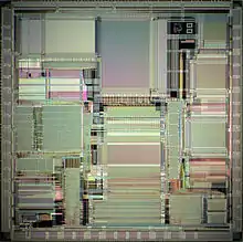
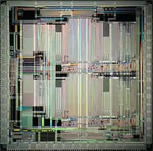
The R8000 contained 2.6 million transistors and measured 17.34 mm by 17.30 mm (299.98 mm²). The R8010 contained 830,000 transistors. In total, the two chips contained 3.43 million transistors. Both were fabricated by Toshiba in their VHMOSIII process, a 0.7 μm, triple-layer metal complementary metal–oxide–semiconductor (CMOS) process. Both are packaged in 591-pin ceramic pin grid array (CPGA) packages. Both chips used a 3.3 V power supply, and the R8000 dissipated 13 W at 75 MHz.
Notes
- Hsu 1994
- Dongarra 1994
- MIPS Technologies, Inc., 1994
- MIPS 1994
- Unekawa 1993
References
- "Aligning Instructions for Multiple Dispatch". Sidebar in Pountain, Dick, "The Last Bastion", Byte, August 1994.
- Dongarra, Jack J.; Meuer, Hans W. and Strohmaier, Erich (9 November 1994). TOP500 Supercomputer Sites.
- Gwennap, Linley (15 February 1993). "SGI Provides Overview of TFP CPU". Microprocessor Report, vol. 7, no. 2.
- Gwennap, Linley (23 August 1993). "TFP Designed for Tremendous Floating Point". Microprocessor Report, vol. 7, no. 11.
- Hsu, Peter Yan-Tek (2 June 1994). Design of the R8000 Microprocessor.
- MIPS Technologies, Inc. (August 1994). R8000 Microprocessor Chip Set Product Overview.
- Pountain, Dick (September 1994). "The Last Bastion". Byte.
- Shen, John Paul; Lipasti, Mikko H. (2005). Modern Processor Design: Fundamentals of Superscalar Microprocessors. McGraw-Hill Professional. pp. 418–419.
- Unekawa, Yasuo et al. (1993). "A 110MHz / 1Mbit synchronous Tag RAM". Symposium on VLSI Circuits. pp. 15–16.
Further reading
- Ikumi, N. et al. (February 1994). "A 300 MIPS, 300 MFLOPS four-issue CMOS superscalar microprocessor". ISSCC Digest of Technical Papers.
- Unekawa, Y. et al. (April 1994). "A 110-MHz/1-Mb synchronous TagRAM". IEEE Journal of Solid-State Circuits 29 (4): pp. 403–410.
- How VLIW almost disappeared
- Peter Hsu Design of the R8000 IEEE Micro 1994