R10000
The R10000, code-named "T5", is a RISC microprocessor implementation of the MIPS IV instruction set architecture (ISA) developed by MIPS Technologies, Inc. (MTI), then a division of Silicon Graphics, Inc. (SGI). The chief designers are Chris Rowen and Kenneth C. Yeager. The R10000 microarchitecture is known as ANDES, an abbreviation for Architecture with Non-sequential Dynamic Execution Scheduling. The R10000 largely replaces the R8000 in the high-end and the R4400 elsewhere. MTI was a fabless semiconductor company; the R10000 was fabricated by NEC and Toshiba. Previous fabricators of MIPS microprocessors such as Integrated Device Technology (IDT) and three others did not fabricate the R10000 as it was more expensive to do so than the R4000 and R4400.

History
The R10000 was introduced in January 1996 at clock frequencies of 175 MHz and 195 MHz. A 150 MHz version was introduced in the O2 product line in 1997, but discontinued shortly after due to customer preference for the 175 MHz version. The R10000 was not available in large volumes until later in the year due to fabrication problems at MIPS's foundries. The 195 MHz version was in short supply throughout 1996, and was priced at US$3,000 as a result.[1]
On 25 September 1996, SGI announced that R10000s fabricated by NEC between March and the end of July that year were faulty, drawing too much current and causing systems to shut down during operation. SGI recalled 10,000 R10000s that had shipped in systems as a result, which impacted the company's earnings.
In 1997, a version of R10000 fabricated in a 0.25 µm process enabled the microprocessor to reach 250 MHz.
Users
Users of the R10000 include:
- SGI:
- NEC, in its Cenju-4 supercomputer
- Siemens Nixdorf, in its servers run under SINIX
- Tandem Computers, in its Himalaya fault-tolerant servers
Description

The R10000 is a four-way superscalar design that implements register renaming and executes instructions out-of-order. Its design is a departure from previous MTI microprocessors such as the R4000, which is a much simpler scalar in-order design that relies largely on high clock rates for performance.
The R10000 fetches four instructions every cycle from its instruction cache. These instructions are decoded and then placed into the integer, floating-point or load/store instruction queues depending on the type of the instruction. The decode unit is assisted by the pre-decoded instructions from the instruction cache, which append five bits to every instruction to enable the unit to quickly identify which execution unit the instruction is executed in, and rearrange the format of the instruction to optimize the decode process.
Each of the instruction queues can accept up to four instructions from the decoder, avoiding any bottlenecks. The instruction queues issue their instructions to their execution units dynamically depending on the availability of operands and resources. Each of the queues except for the load/store queue can issue up to two instructions every cycle to its execution units. The load/store queue can only issue one instruction. The R10000 can thus issue up to five instructions every cycle.
Integer unit
The integer unit consists of the integer register file and three pipelines, two integer, one load store. The integer register file is 64 bits wide and contains 64 entries, of which 32 are architectural registers and 32 are rename registers which implement register renaming. The register file has seven read ports and three write ports. Both integer pipelines have an adder and a logic unit. However, only the first pipeline has a barrel shifter and hardware for confirming the prediction of conditional branches. The second pipeline is used to access the multiplier and divider. Multiplies are pipelined, and have a six-cycle latency for 32-bit integers and ten for 64-bit integers. Division is not pipelined. The divider uses a non-restoring algorithm that produces one bit per cycle. Latencies for 32-bit and 64-bit divides are 35 and 67 cycles, respectively.
Floating-point unit
The floating-point unit (FPU) consists of four functional units, an adder, a multiplier, divide unit and square root unit. The adder and multiplier are pipelined, but the divide and square root units are not. Adds and multiplies have a latency of three cycles and the adder and multiplier can accept a new instruction every cycle. The divide unit has a 12- or 19-cycle latency, depending on whether the divide is single precision or double precision, respectively.
The square root unit executes square root and reciprocal square root instructions. Square root instructions have an 18- or 33-cycle latency for single precision or double precision, respectively. A new square root instruction can be issued to the divide unit every 20 or 35 cycles for single precision and double precision respectively. Reciprocal square roots have longer latencies, 30 to 52 cycles for single precision (32-bit) and double precision (64-bit) respectively.
The floating-point register file contains sixty-four 64-bit registers, of which thirty-two are architectural and the remaining are rename registers. The adder has its own dedicated read and write ports, whereas the multiplier shares its with the divider and square root unit.
The divide and square root units use the SRT algorithm. The MIPS IV ISA has a multiply–add instruction. This instruction is implemented by the R10000 with a bypass — the result of the multiply can bypass the register file and be delivered to the add pipeline as an operand, thus it is not a fused multiply–add, and has a four-cycle latency.
Caches
The R10000 has two comparatively large on-chip caches, a 32 KB instruction cache and a 32 KB data cache. The instruction cache is two-way set-associative and has a 128-byte line size. Instructions are partially decoded by appending four bits to each instruction (which have a length of 32 bits) before they are placed in the cache.
The 32 KB data cache is dual-ported through two-way interleaving. It consists of two 16 KB banks, and each bank are two-way set-associative. The cache has 64-byte lines, uses the write-back protocol, and is virtually indexed and physically tagged to enable the cache to be indexed in the same clock cycle and to maintain coherency with the secondary cache.
The external secondary unified cache supported capacities between 512 KB and 16 MB. It is implemented with commodity synchronous static random access memorys (SSRAMs). The cache is accessed via its own 128-bit bus that is protected by 9-bits of error correcting code (ECC). The cache and bus operate at the same clock rate as the R10000, whose maximum frequency was 200 MHz. At 200 MHz, the bus yielded a peak bandwidth of 3.2 GB/s. The cache is two-way set associative, but to avoid a high pin count, the R10000 predicts which way is accessed.
Addressing
MIPS IV is a 64-bit architecture, but to reduce cost the R10000 does not implement the entire physical or virtual address. Instead, it has a 40-bit physical address and a 44-bit virtual address, thus it is capable of addressing 1 TB of physical memory and 16 TB of virtual memory.
Avalanche system bus
The R10000 uses the Avalanche bus, a 64-bit bus that operates at frequencies up to 100 MHz. Avalanche is a multiplexed address and data bus, so at 100 MHz it yields a maximum theoretical bandwidth of 800 MB/s, but its peak bandwidth is 640 MB/s as it requires some cycles to transmit addresses.
The system interface controller supports glue-less symmetrical multiprocessing (SMP) of up to four microprocessors. Systems using the R10000 with external logic can scale to hundreds of processors. An example of such a system is the Origin 2000.
Fabrication
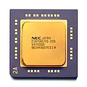
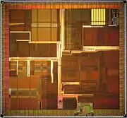
The R10000 consists of approximately 6.8 million transistors, of which approximately 4.4 million are contained in the primary caches.[2] The die measures 16.640 by 17.934 mm, for a die area of 298.422 mm2. It is fabricated in a 0.35 µm process and packaged in 599-pad ceramic land grid array (LGA). Before the R10000 was introduced, the Microprocessor Report, covering the 1994 Microprocessor Forum, reported that it was packaged in a 527-pin ceramic pin grid array (CPGA); and that vendors also investigated the possibility of using a 339-pin multi-chip module (MCM) containing the microprocessor die and 1 MB of cache.[3]
Derivatives
The R10000 was extended by multiple successive derivatives. All derivatives after the R12000 have their clock frequency kept as low as possible to maintain power dissipation in the 15 to 20 W range so they can be densely packaged in SGI's high performance computing (HPC) systems.
R12000

The R12000 is a derivative of the R10000 started by MIPS and completed by SGI. It was fabricated by NEC and Toshiba. The version fabricated by NEC is called the VR12000. The microprocessor was introduced in November 1998. It is available at 270, 300 and 360 MHz. The R12000 was developed as a stop-gap solution following the cancellation of the "Beast" project, which intended to deliver a successor to the R10000. R12000 users include NEC, Siemens-Nixdorf, SGI and Tandem Computers (and later Compaq, after their acquisition of Tandem).
The R12000 improves upon the R10000 microarchitecture by: inserting an extra pipeline stage to improve clock frequency by resolving a critical path; increasing the number of entries in the branch history table, improving prediction; modifying the instruction queues so they take into account the age of a queued instruction, enabling older instructions to be executed before newer ones if possible.
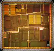
The R12000 was fabricated by NEC and Toshiba in a 0.25 µm CMOS process with four levels of aluminum interconnect. The use of a new process does not mean that the R12000 was a simple die shrink with a tweaked microarchitecture; the layout of the die is optimized to take advantage of the 0.25 µm process.[4][5] The NEC fabricated VR12000 contained 7.15 million transistors and measured 15.7 by 14.6 mm (229.22 mm2).
R12000A
The R12000A is a derivative of the R12000 developed by SGI. Introduced in July 2000, it operates at 400 MHz and was fabricated by NEC a 0.18 µm process with aluminum interconnects.
R14000
The R14000 is a further development of the R12000 announced in July 2001. The R14000 operates at 500 MHz, enabled by the 0.13 µm CMOS process with five levels of copper interconnect it is fabricated with. It features improvements to the microarchitecture of the R12000 by supporting double data rate (DDR) SSRAMs for the secondary cache and a 200 MHz system bus.[6]
R14000A
The R14000A is a further development of the R14000 announced in February 2002. It operates at 600 MHz, dissipates approximately 17 W, and was fabricated by NEC Corporation in a 0.13 µm CMOS process with seven levels of copper interconnect.[6]
R16000
The R16000, code-named "N0", is the last derivative of the R10000. It is developed by SGI and fabricated by NEC in their 0.11 µm process with eight levels of copper interconnect. The microprocessor was introduced on 9 January 2003, debuting at 700 MHz for the Fuel and also used in their Onyx4 Ultimate Vision.[7] In April 2003, a 600 MHz version was introduced for the Origin 350. Improvements are 64 KB instruction and data caches.
R16000A
The R16000A refers to R16000 microprocessors with clock rates higher than 700 MHz. The first R16000A is an 800 MHz version, introduced on 4 February 2004. Later, a 900 MHz version was introduced, and this version was, for some time, the fastest publicly known R16000A—SGI later revealed there were 1.0 GHz R16000s shipped to selected customers. R16000 users included HP and SGI. SGI used the microprocessor in their Fuel and Tezro workstations; and the Origin 3000 servers and supercomputers. HP used the R16000A in their NonStop Himalaya S-Series fault-tolerant servers inherited from Tandem via Compaq.
R18000
The R18000 is a canceled further development of the R10000 microarchitecture that featured major improvements by Silicon Graphics, Inc. described at the Hot Chips symposium in 2001. The R18000 was designed specifically for SGI's ccNUMA servers and supercomputers. Each node would have two R18000s connected via a multiplexed bus to a system controller, which would interface the microprocessors to their local memory and the rest of the system via a hypercube network.
The R18000 improved the floating-point instruction queues and revised the floating-point unit to feature two multiply–add units, quadrupling the peak FLOPS count. Division and square-root would be performed in separate non-pipelined units in parallel to the multiply–add units. The system interface and memory hierarchy was also significantly reworked. It would have a 52-bit virtual address and a 48-bit physical address. The bidirectional multiplexed address and data system bus of the earlier models would be replaced by two unidirectional DDR links, a 64-bit multiplexed address and write path and a 128-bit read path. The paths could be shared with another R18000 through multiplexing. The bus could also be configured in the SysAD or Avalanche configuration for backwards compatibility with R10000 systems.
The R18000 would have a 1 MB four-way set-associative secondary cache to be included on-die; supplemented by an optional tertiary cache built from single data rate (SDR) or double data rate (DDR) SSRAM or DDR SDRAM with capacities of 2 to 64 MB. The L3 cache would have its cache tags, equivalent to 400 KB, located on-die to reduce latency. The L3 cache would be accessed via a 144-bit bus, of which 128 bits are for data and 16 bits for ECC. The L3 cache's clock rate would be programmable.
The R18000 was to be fabricated in NEC's UX5 process, a 0.13 µm CMOS process with nine levels of copper interconnect. It would have used 1.2 V power supply and dissipated less heat than contemporary server microprocessors in order to be densely packed into systems.
Notes
- Gwennap, Linley (27 January 1997). "Alpha Sails, PowerPC Flails". Microprocessor Report, pp. 1, 6–9., p. 8."
- Yeager, Kenneth C. (April 1996). "The MIPS R10000 Superscalar Microprocessor" (PDF). IEEE Micro. 16 (2): 28. doi:10.1109/40.491460. Archived from the original (PDF) on 19 July 2011.
- Gwennap, Linley (24 October 1994). "MIPS R10000 Uses Decoupled Architecture" (PDF). Microprocessor Report. 8 (14): 4.
- Gwennap, Linley (6 October 1997). "MIPS R12000 to Hit 300 MHz" (PDF). Microprocessor Report. 11 (13).
- Halfhill, Tom R. (January 1998). "RISC Fights Back with the Mips R12000". Byte. Vol. 23, no. 1. p. 49-50.
- ComputerWire (2 July 2002). "SGI to develop MIPS chips for Origin, Onyx". The Register.
- Silicon Graphics, Inc. (9 January 2003). SGI Boosts Price/Performance on Silicon Graphics Fuel Visual Workstation Family up to 25%. (Press release).
References
- Fu, Tim et al. (31 August 2001). "R18000: The Latest SGI Superscalar Microprocessor". Hot Chips XIII.
- Halfhill, Tom R. (November 1994). "T5: Brute Force". Byte Magazine.
- Heinrich, Joe (29 January 1997). "MIPS R10000 Microprocessor User's Manual".
- Kanellos, Michael; Kawamoto, Dawn (9 April 1998). "Silicon Graphics scraps MIPS plans". CNET News.
- MIPS Technologies, Incorporated. (October 1994). "R10000 Microprocessor Product Review".
- Morgan, Timothy Prickett (16 April 2003). "SGI Announces Origin 350 Midrange HPC Server". IT Jungle.
- NEC Corporation (24 November 1998). NEC Markets World's Highest Class Performance Microprocessor. (Press release).
- Shankland, Stephen (15 April 2003). "SGI updates midrange Unix server". ZDNet.
- Vasseghi, N. et al. (November 1996). "200-MHz superscalar RISC microprocessor". IEEE Journal of Solid-State Circuits 31 (11): pp. 1675–1686.
- Yeager, Kenneth C. (August 1995). "R10000 Superscalar Microprocessor". Hot Chips VII.