Pentium Pro
The Pentium Pro is a sixth-generation x86 microprocessor developed and manufactured by Intel and introduced on November 1, 1995.[1]: D-2 It introduced the P6 microarchitecture (sometimes termed i686) and was originally intended to replace the original Pentium in a full range of applications. While the Pentium and Pentium MMX had 3.1 and 4.5 million transistors, respectively, the Pentium Pro contained 5.5 million transistors.[2]: 12 Later, it was reduced to a more narrow role as a server and high-end desktop processor and was used in supercomputers like ASCI Red, the first computer to reach the trillion floating point operations per second (teraFLOPS) performance mark in 1996.[3] The Pentium Pro was capable of both dual- and quad-processor configurations. It only came in one form factor, the relatively large rectangular Socket 8. The Pentium Pro was succeeded by the Pentium II Xeon in 1998.
 | |
| General information | |
|---|---|
| Launched | November 1, 1995 |
| Discontinued | June 1998 |
| Common manufacturer(s) | |
| Performance | |
| Max. CPU clock rate | 150 MHz to 200 MHz |
| FSB speeds | 60 MHz to 66 MHz |
| Architecture and classification | |
| Technology node | 500 nm to 350 nm |
| Microarchitecture | P6 |
| Instruction set | x86 |
| Physical specifications | |
| Cores |
|
| Socket(s) | |
| History | |
| Predecessor(s) | Pentium |
| Successor(s) | Pentium II, Pentium II Xeon |
| Support status | |
| Unsupported | |
Microarchitecture
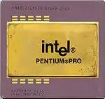
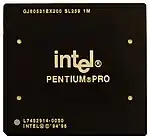
The lead architect of Pentium Pro was Fred Pollack who was specialized in superscalarity and had also worked as the lead engineer of the Intel iAPX 432.[4]
Summary
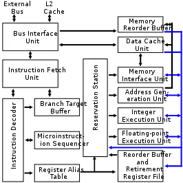
The Pentium Pro incorporated a new microarchitecture, different from the Pentium's P5 microarchitecture. It has a decoupled, 14-stage superpipelined architecture which used an instruction pool. The Pentium Pro (P6) implemented many radical architectural differences mirroring other contemporary x86 designs such as the NexGen Nx586 and Cyrix 6x86. The Pentium Pro pipeline had extra decode stages to dynamically translate IA-32 instructions into buffered micro-operation sequences which could then be analysed, reordered, and renamed in order to detect parallelizable operations that may be issued to more than one execution unit at once. The Pentium Pro thus featured out of order execution, including speculative execution via register renaming. It also had a wider 36-bit address bus, usable by Physical Address Extension (PAE), allowing it to access up to 64 GB of memory.
The Pentium Pro has an 8 KB instruction cache, from which up to 16 bytes are fetched on each cycle and sent to the instruction decoders. There are three instruction decoders. The decoders are unequal in ability: only one can decode any x86 instruction, while the other two can only decode simple x86 instructions. This restricts the Pentium Pro's ability to decode multiple instructions simultaneously, limiting superscalar execution. x86 instructions are decoded into 118-bit micro-operations (micro-ops). The micro-ops are reduced instruction set computer (RISC)-like; that is, they encode an operation, two sources, and a destination. The general decoder can generate up to four micro-ops per cycle, whereas the simple decoders can generate one micro-op each per cycle. Thus, x86 instructions that operate on the memory (e.g., add this register to this location in the memory) can only be processed by the general decoder, as this operation requires a minimum of three micro-ops. Likewise, the simple decoders are limited to instructions that can be translated into one micro-op. Instructions that require more micro-ops than four are translated with the assistance of a sequencer, which generates the required micro-ops over multiple clock cycles. The Pentium Pro was the first processor in the x86-family to support upgradeable microcode under BIOS and/or operating system (OS) control.[5]
Micro-ops exit the re-order buffer (ROB) and enter a reserve station (RS), where they await dispatch to the execution units. In each clock cycle, up to five micro-ops can be dispatched to five execution units. The Pentium Pro has a total of six execution units: two integer units, one floating-point unit (FPU), a load unit, store address unit, and a store data unit.[6] One of the integer units shares the same ports as the FPU, and therefore the Pentium Pro can only dispatch one integer micro-op and one floating-point micro-op, or two integer micro-ops per a cycle, in addition to micro-ops for the other three execution units. Of the two integer units, only the one that shares the path with the FPU on port 0 has the full complement of functions such as a barrel shifter, multiplier, divider, and support for LEA instructions. The second integer unit, which is connected to port 1, does not have these facilities and is limited to simple operations such as add, subtract, and the calculation of branch target addresses.[6]
The FPU executes floating-point operations. Addition and multiplication are pipelined and have a latency of three and five cycles, respectively. Division and square-root are not pipelined and are executed in separate units that share the FPU's ports. Division and square root have a latency of 18-36 and 29-69 cycles, respectively. The smallest number is for single precision (32-bit) floating-point numbers and the largest for extended precision (80-bit) numbers. Division and square root can operate simultaneously with adds and multiplies, preventing them from executing only when the result has to be stored in the ROB.
After the microprocessor was released, a bug was discovered in the floating point unit, commonly called the "Pentium Pro and Pentium II FPU bug" and by Intel as the "flag erratum". The bug occurs under some circumstances during floating point-to-integer conversion when the floating point number will not fit into the smaller integer format, causing the FPU to deviate from its documented behaviour. The bug is considered to be minor and occurs under such special circumstances that very few, if any, software programs are affected.
The Pentium Pro P6 microarchitecture was used in one form or another by Intel for more than a decade. The pipeline would scale from its initial 150 MHz start, all the way up to 1.4 GHz with the "Tualatin" Pentium III. The design's various traits would continue after that in the derivative core called "Banias" in Pentium M and Intel Core (Yonah), which itself would evolve into the Core microarchitecture (Core 2 processor) in 2006 and onward.[7]
Instruction set
The Pentium Pro (P6) introduced new instructions into the Intel range; the CMOVxx (‘conditional move’) instructions can move a value that is either the contents of a register or memory location into another register or not, according to some predicate logical condition xx on the flags register, xx being a flags predicate code as given in the condition for conditional jump instructions. So for example CMOVNE moves a specified value into a register or not depending on whether the NE (not-equal) condition is true in the flags register ie Z flag = 0. This allows the evaluation of if-then-else operations and for example the ? : operation in C. These instructions give a performance boost by allowing the avoidance of costly jump and branch instructions. In eg CMOVxx destreg1, source_operand2 the first operand is the destination register, the second the source register or memory location. The second operand unfortunately can not be an immediate (in-line constant) value and such a constant would have to be placed in a register first. The predicate code xx can take the full range of values as allowed in conditional branches.
A second development was the documentation of the UD2 illegal instruction. This op code is reserved and guaranteed to cause an illegal instruction exception on the P6 and all later processors. This allows developers to easily crash the current program in a future-proof fashion when a bug is detected by software.
Performance
Despite being advanced for the time, the Pentium Pro's out-of-order register renaming architecture had trouble running 16-bit code and mixed code (8-bit with 16-bit (8/16), or 16-bit with 32-bit (16/32), as using partial registers cause frequent pipeline flushing.[8] Specific use of partial registers was then a common performance optimization, as it incurred no performance penalty on pre-P6 Intel processors; also, the dominant operating systems at the time of the Pentium Pro's release were 16-bit DOS, and mixed 16/32-bit Windows 3.1x and Windows 95 (although the latter requires a 32-bit 80386 CPU, much of its code is still 16-bit for performance reasons, such as USER.exe). This, with the high cost of Pentium Pro systems, led to tepid sales among PC buyers at the time. To fully use the Pentium Pro's P6 microarchitecture, a fully 32-bit operating system is needed, such as Windows NT, Linux, Unix, or OS/2. The performance issues on legacy code were later partly mitigated by Intel with the Pentium II.
Compared to RISC microprocessors, the Pentium Pro, when introduced, slightly outperformed the fastest RISC microprocessors on integer performance when running the SPECint95 benchmark,[9]: 2 but floating-point performance was significantly lower, half that of some RISC microprocessors.[9]: 3 The Pentium Pro's integer performance lead disappeared rapidly, first overtaken by the MIPS Technologies R10000 in January 1996, and then by Digital Equipment Corporation's EV56 variant of the Alpha 21164.[10]
Reviewers quickly noted the very slow writes to video memory as the weak spot of the P6 platform, with performance here being as low as 10% of an identically clocked Pentium system in benchmarks such as VIDSPEED. Methods to circumvent this included setting VESA drawing to system memory instead of video memory in games such as Quake,[11] and later on utilities such as FASTVID emerged, which could double performance in certain games by enabling the write combining features of the CPU.[12][13] memory type range registers (MTRRs) are set automatically by Windows video drivers starting from ~1997, and there the improved cache/memory subsystem and FPU performance caused it to outclass the Pentium clock-for-clock in the emerging 3D games of the mid–to–late 1990s, particularly when using NT4. However, its lack of MMX implementation reduces performance in multimedia applications that made use of those instructions.
Caching
Likely Pentium Pro's most noticeable addition was its on-package L2 cache, which ranged from 256 KB at introduction to 1 MB in 1997. At the time, manufacturing technology did not feasibly allow a large L2 cache to be integrated into the processor core. Intel instead placed the L2 die(s) separately in the package which still allowed it to run at the same clock speed as the CPU core. Additionally, unlike most motherboard-based cache schemes that shared the main system bus with the CPU, the Pentium Pro's cache had its own back-side bus (called dual independent bus by Intel). Because of this, the CPU could read main memory and cache concurrently, greatly reducing a traditional bottleneck.[14] The cache was also "non-blocking", meaning that the processor could issue more than one cache request at a time (up to 4), reducing cache-miss penalties. (This is an example of MLP, Memory Level Parallelism.) These properties combined to produce an L2 cache that was immensely faster than the motherboard-based caches of older processors. This cache alone gave the CPU an advantage in input/output performance over older x86 CPUs. In multiprocessor configurations, Pentium Pro's integrated cache skyrocketed performance in comparison to architectures which had each CPU sharing a central cache.
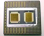
However, this far faster L2 cache did come with some complications. The Pentium Pro's "on-package cache" arrangement was unique. The processor and the cache were on separate dies in the same package and connected closely by a full-speed bus. The two or three dies had to be bonded together early in the production process, before testing was possible. This meant that a single, tiny flaw in either die made it necessary to discard the entire assembly, which was one of the reasons for the Pentium Pro's relatively low production yield and high cost. All versions of the chip were expensive, those with 1024 KB being particularly so, since it required two 512 KB cache dies as well as the processor die.
Available models
Pentium Pro clock speeds were 150, 166, 180 or 200 MHz with a 60 or 66 MHz external bus clock. Some users chose to overclock their Pentium Pro chips, with the 200 MHz version often being run at 233 MHz, the 180 MHz version often being run at 200 MHz, and the 150 MHz version often being run at 166 MHz. The chip was popular in symmetric multiprocessing configurations, with dual and quad SMP server and workstation setups being commonplace.
Intel skipped out on providing a mobile version of the original Pentium Pro due to power draw and heat concerns.[15] At least one vendor sold a portable computer with a Pentium Pro (Imperial Computer's 6200TLP).[16]
In Intel's "Family/Model/Stepping" scheme, the Pentium Pro is family 6, model 1, and its Intel Product code is 80521.
| Clock | Bus | L2-Cache | Max TDP |
|---|---|---|---|
| 150 MHz | 60 MHz | 256 KB | 29.2 W |
| 166 MHz | 66 MHz | 512 KB | 35 W |
| 180 MHz | 60 MHz | 256 KB | 31.7 W |
| 200 MHz | 66 MHz | 35 W | |
| 512 KB | 37.9 W | ||
| 1024 KB | 44 W |
Fabrication
The process used to fabricate the Pentium Pro processor die and its separate cache memory die changed, leading to a combination of processes used in the same package:
- The 133 MHz Pentium Pro prototype processor die was fabricated in a 0.6 μm BiCMOS process.[17][18]
- The 150 MHz Pentium Pro processor die was fabricated in a 0.50 μm BiCMOS process.[18][9]
- The 166, 180, and 200 MHz Pentium Pro processor die was fabricated in a 0.35 μm BiCMOS process.[18][9]
- The 256 KB L2 cache die was fabricated in a 0.50 μm BiCMOS process.[18][9]
- The 512 and 1024 KB L2 cache die was fabricated in a 0.35 μm BiCMOS process.[18][9]
Packaging
The Pentium Pro (up to 512 KB cache) is packaged in a ceramic multi-chip module (MCM). The MCM contains two underside cavities in which the microprocessor die and its companion cache die reside. The dies are bonded to a heat slug, whose exposed top helps the heat from the dies to be transferred more directly to cooling apparatus such as a heat sink. The dies are connected to the package using conventional wire bonding. The cavities are capped with a ceramic plate.
The Pentium Pro with 1 MB of cache uses a plastic MCM. Instead of two cavities, there is only one, in which the three dies reside, bonded to the package instead of a heat slug. The cavities are filled in with epoxy.
The MCM has 387 pins, of which approximately half are arranged in a pin grid array (PGA) and half in an interstitial pin grid array (IPGA). The packaging was designed for Socket 8.
Upgrade paths
In 1998, the 300/333 MHz Pentium II Overdrive processor for Socket 8 was released. Featuring double L1 and 512 KB of full-speed L2 cache, it was produced by Intel as a drop-in upgrade option for owners of Pentium Pro systems. However, it only supported two-way glueless multiprocessing, not four-way or higher, which did not make it a usable upgrade for quad-processor systems. These specially packaged Pentium II Xeon processors were also used to upgrade ASCI Red, which became the first computer to reach the teraFLOPS performance mark with the Pentium Pro processor in 1996 and then the first to exceed 2 teraFLOPS after the upgrade to Pentium II Xeon processors in 1999.
As Slot 1 motherboards became prevalent, several manufacturers released slocket adapters, such as the Tyan M2020, Asus C-P6S1, Tekram P6SL1, and the Abit KP6. The sockets allowed Pentium Pro processors to be used with Slot 1 motherboards. The Intel 440FX chipset explicitly supported both Pentium Pro and Pentium II processors, but the Intel 440BX and later Slot 1 chipsets did not explicitly support the Pentium Pro, so the Socket 8 slockets did not see wide use. Slockets, in the form of Socket 370 to Slot 1 adapters, saw renewed popularity when Intel introduced Socket 370 Celeron and Pentium III processors.
Core specifications
Pentium Pro
- L1 cache: 8, 8 KB (data, instructions)
- L2 cache: 256, 512 KB (one die) or 1024 KB (two 512 KB dies) in a multi-chip module clocked at CPU-speed
- Socket: Socket 8
- Front-side bus: 60 and 66 MHz
- VCore: 3.1–3.3 V
- Fabrication: 0.50 μm or 0.35 BiCMOS[19]
- Clockrate: 150, 166, 180, 200 MHz, (capable of 233 MHz on some motherboards)
- First release: November 1995
Pentium II Overdrive
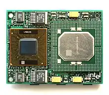
- L1 cache: 16, 16 KB (data + instructions)
- L2 cache: 512 KB external chip on CPU module clocked at CPU-speed
- Socket: Socket 8
- Multiplier: Locked at 5×
- Front-side bus: 60 and 66 MHz
- VCore: 3.1–3.3 V (has on-board voltage regulator)
- Fabrication: 0.25 μm
- Clockrate: Based on the Deschutes-generation Pentium II
- First release: 1997
- Supports MMX technology
Bus and multiprocessor capabilities
The Pentium Pro used GTL+ signaling in its front-side bus.[21] The Pentium Pro could be used by itself on up to four-way designs. Eight-way Pentium Pro computers were also built, but these used multiple buses.[22]
The design of the Pentium Pro bus was influenced by Futurebus, the Intel iAPX 432 bus, and elements of the Intel i960 bus.[23] Futurebus has been intended as an advanced bus to replace VMEbus used with the Motorola 68000 from the late 1970s, but it stagnated in standardization committee for more than a decade if you count all the twists and turns.[23] Intel's iAPX 432 initiative was also a commercial failure, but in the process they did learn how to build a split-transaction bus to support a cacheless multiprocessor system. The i960 had further developed the split-transaction iAPX 432 bus to include a cache coherency protocol, ending up with a feature set highly reminiscent of the original Futurebus ambitions.[23]
The lead architect of i960 was superscalarity specialist Fred Pollack who was also the lead engineer of the Intel iAPX 432 and the lead architect of the i686 chip, the Pentium Pro. He was no doubt intimately familiar with all this history. The Pentium Pro was designed to include the 4-way SMP split-transaction cache-coherent bus as a mandatory feature of every chip produced.[23] This also served to deny competition access to the socket to produce cloned processors.[23]
While the Pentium Pro was not successful as a machine for the masses, due to poor 16-bit support for Windows 95, it did become highly successful in the file server space due to its advanced, integrated bus design,[23] introducing many advanced features that had formerly only been available in the pricey workstation segment into the commodity marketplace.
Pentium Pro/6th generation competitors
References
- Fisher, Lawrence M. (2 November 1995). "Intel Offers Its Pentium Pro For Work Station Market". The New York Times (New York ed.). p. D-2. eISSN 1553-8095. ISSN 0362-4331. Archived from the original on 4 August 2009. Retrieved 28 December 2022.
The Intel Corporation today introduced its new microprocessor, the Pentium Pro. But although the chip's performance is higher than expected, and its price lower, analysts said its immediate impact was not likely to match that of its predecessor, the Pentium.
- Brey, Barry B. (2003). "Introduction to the Microprocessor and Computer". The Intel Microprocessors 8086/8088, 80186, 80286, 80386, 80486: Architecture, Programming, and Interfacing (Sixth (International) ed.). Pearson Education. p. 12. ISBN 978-0130487209. LCCN 93021801. OCLC 224097450. OL 1412841M. Retrieved 15 December 2022.
- "ASCI Red: Sandia National Laboratory". TOP500. n.d. Retrieved January 7, 2023.
Intel's ASCI Red supercomputer was the first teraflop/s computer, taking the No.1 spot on the 9th TOP500 list in June 1997 with a Linpack performance of 1.068 teraflop/s. [...] It was a mesh-based (38 X 32 X 2) MIMD massively parallel machine initially consisting of 7,264 compute nodes, 1,212 gigabytes of total distributed memory and 12.5 terabytes of disk storage. The original incarnation of this machine used Intel Pentium Pro processors, each clocked at 200 MHz. These were later upgraded to Pentium II OverDrive processors. The system was upgraded to a total of 9,632 Pentium II Over-Drive processors, each clocked at 333 MHz.
- Dvorak, John C. (25 November 2006). "Whatever Happened to The iAPX432 – Intel's Dream Chip?". Dvorak Uncensored. Archived from the original on 13 December 2008. Retrieved 28 December 2022.
There were a lot of pieces involved in this chip but today's Pentium Pro consists of two chips and other needed support chips too. Curiously the lead engineer for the 432 was superstar designer Fred Pollack who became the lead architect for the Pentium Pro.
- Stiller, Andreas; Paul, Matthias R. (12 May 1996). "Trends & News | Prozessorgeflüster" [Trends & News | Processor whisper]. c't | magazin für computertechnik (in German). Heinz Heise. ISSN 0724-8679. OCLC 314471122. Archived from the original on 28 December 2022. Retrieved 28 December 2022.
Offenbar hat der PPro einen ladbaren Microcode, für den das Board-BIOS zwei Funktionen im Interrupt 15h zum Auslesen und Laden bereithält (näheres im nächsten Update der Interrupt-Liste). Gedacht ist das für Patches, doch wer weiß, welch ungeahnte Möglichkeiten noch darinstecken. Somit hat man es beim PPro in Zukunft nicht nur mit zwei Masken-Versionen (für CPU und Cache), sondern auch noch mit der Update-Version des Microcode-BIOS zu tun (zum Beispiel beim aktuellen 200-MHz-'P6S' mit der Kennung SY013: CPU-Step A0, Cache-Step B1, BIOS: sA0C05).
[Apparently the PPro has a loadable microcode, for which the board BIOS provides two functions in interrupt 15h for reading and loading (more information in the next update of the interrupt list). This is intended for patches, but who knows what undreamt-of possibilities are still there. In the future, therefore, the PPro will not only have to deal with two mask versions (for CPU and cache), but also with the update version of the microcode BIOS (e.g. with the current 200 MHz 'P6S' with the Identifier SY013: CPU step A0, cache step B1, BIOS: sA0C05).] - "Intel Architecture Optimization Manual" (PDF). 1997. p. 2-8. Archived from the original (PDF) on January 21, 2007.
- Stokes, Jon (5 April 2006). "Into the Core: Intel's next-generation microarchitecture". Tech. Ars Technica. OCLC 52157687. Archived from the original on 18 December 2022. Retrieved 28 December 2022.
The P6 lineage from the Pentium Pro to the Pentium M [...] One of the most distinctive features of the P6 line is its issue port structure. (Intel calls these "dispatch ports," but for the sake of consistency with the rest of my work I'll be using the terms "dispatch" and "issue" differently than Intel.) Core uses a similar structure in its execution core, although there are some major differences between Core's issue port and RS combination and that of the P6.
- "Partial Register Stall Warning". VTune Performance Analyzer online help. Archived from the original on August 30, 2017.
- Slater, Michael (13 November 1995). "Intel Boosts Pentium Pro to 200 MHz" (PDF). Microprocessor Report. MicroDesign Resources. Vol. 9, no. 15. Archived (PDF) from the original on 2 December 2021. Retrieved 28 December 2022 – via Ardent Tool of Capitalism (ardent-tool.com).
Integer Leads, FP Lags RISC Chips
- Gwennap, Linley (July 8, 1996). "Digital's 21164 Reaches 500 MHz". Microprocessor Report.
- "Quake/TECHINFO.TXT at master · id-Software/Quake". GitHub. November 25, 2022.
- "Quake Technical Information file".
- "MDGx Complete UMBPCI.SYS Guide". MDGx MAX Speed WinDOwS Tricks + Secrets. Fast Video.
- "Accelerated Graphics Port". Next Generation. No. 37. Imagine Media. January 1998. pp. 94–96.
- April, Carolyn A. (December 16, 1996). "Intel postpones Pentium Pro notebook drive". InfoWorld. IDG Publications. 18 (51): 14 – via Google Books.
- O'Brien, Bill (November 1996). "Pentium Pro built to go". Computer Shopper. SX2 Media Labs. 16 (11): 420 – via Gale.
- Papworth, David B. (April 1996). "Tuning the Pentium Pro Microarchitecture". IEEE Micro, pp. 14–15.
- "Intel Pentium Pro Processors - Fact Sheet". Intel. Archived from the original on December 7, 2013.
- sandpile.org Archived September 1, 1999, at archive.today - IA-32 implementation - Intel P6
- Schnurer, Georg. "Next Exit: Mendocino". Archived from the original on February 19, 2006. Retrieved April 24, 2009.
- Shanley, Tom (1998). Pentium Pro and Pentium II System Architecture. Addison-Wesley Professional. p. 199. ISBN 978-0-201-30973-7.
- Guruge, Anura (May 17, 2000). Web-to-Host Connectivity. CRC Press. p. 405. ISBN 978-0-203-99747-5.
- Hardenberg, Hal W. (June 1, 1997). "Back to the Futurebus". drdobbs.com. Dr. Dobb's Journal. Retrieved September 19, 2020.
External links
- Backside Bus, searchstorage.techtarget.com
- Intel Pentium Pro images and descriptions, cpu-collection.de
- CPU-INFO: Intel Pentium Pro, indepth processor history, web.archive.org