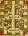
Die shrink
The term die shrink (sometimes optical shrink or process shrink) refers to the scaling of metal–oxide–semiconductor (MOS) devices. The act of shrinking a die creates a somewhat identical circuit using a more advanced fabrication process, usually involving an advance of lithographic nodes. This reduces overall costs for a chip company, as the absence of major architectural changes to the processor lowers research and development costs while at the same time allowing more processor dies to be manufactured on the same piece of silicon wafer, resulting in less cost per product sold.
| Semiconductor device fabrication |
|---|
 |
|
MOSFET scaling (process nodes) |
|
Future
|
Die shrinks are the key to lower prices and higher performance at semiconductor companies such as Samsung, Intel, TSMC, and SK Hynix, and fabless manufacturers such as AMD (including the former ATI), NVIDIA and MediaTek.
Details
Examples in the 2000s include the downscaling of the PlayStation 2's Emotion Engine processor from Sony and Toshiba (from 180 nm CMOS in 2000 to 90 nm CMOS in 2003),[1] the codenamed Cedar Mill Pentium 4 processors (from 90 nm CMOS to 65 nm CMOS) and Penryn Core 2 processors (from 65 nm CMOS to 45 nm CMOS), the codenamed Brisbane Athlon 64 X2 processors (from 90 nm SOI to 65 nm SOI), various generations of GPUs from both ATI and NVIDIA, and various generations of RAM and flash memory chips from Samsung, Toshiba and SK Hynix. In January 2010, Intel released Clarkdale Core i5 and Core i7 processors fabricated with a 32 nm process, down from a previous 45 nm process used in older iterations of the Nehalem processor microarchitecture. Intel, in particular, formerly focused on leveraging die shrinks to improve product performance at a regular cadence through its Tick-Tock model. In this business model, every new microarchitecture (tock) is followed by a die shrink (tick) to improve performance with the same microarchitecture.[2]
Die shrinks are beneficial to end-users as shrinking a die reduces the current used by each transistor switching on or off in semiconductor devices while maintaining the same clock frequency of a chip, making a product with less power consumption (and thus less heat production), increased clock rate headroom, and lower prices.[2] Since the cost to fabricate a 200-mm or 300-mm silicon wafer is proportional to the number of fabrication steps and not proportional to the number of chips on the wafer, die shrinks cram more chips onto each wafer, resulting in lowered manufacturing costs per chip.
Half-shrink
In CPU fabrications, a die shrink always involves an advance to a lithographic node as defined by ITRS (see list). For GPU and SoC manufacturing, the die shrink often involves shrinking the die on a node not defined by the ITRS, for instance, the 150 nm, 110 nm, 80 nm, 55 nm, 40 nm and more currently 8 nm nodes, sometimes referred to as "half-nodes". This is a stopgap between two ITRS-defined lithographic nodes (thus called a "half-node shrink") before further shrink to the lower ITRS-defined nodes occurs, which helps save additional R&D cost. The choice to perform die shrinks to either full nodes or half-nodes rests with the foundry and not the integrated circuit designer.
| Main ITRS node | Stopgap half-node |
|---|---|
| 250 nm | 220 nm |
| 180 nm | 150 nm |
| 130 nm | 110 nm |
| 90 nm | 80 nm |
| 65 nm | 55 nm |
| 45 nm | 40 nm |
| 32 nm | 28 nm |
| 22 nm | 20 nm |
| 14 nm | 12 nm[3] |
| 10 nm | 8 nm |
| 7 nm | 6 nm |
| 5 nm | 4 nm |
| 3 nm | — |
See also
References
- "EMOTION ENGINE® AND GRAPHICS SYNTHESIZER USED IN THE CORE OF PLAYSTATION® BECOME ONE CHIP" (PDF). Sony. April 21, 2003. Retrieved 26 June 2019.
- "Intel's 'Tick-Tock' Seemingly Dead, Becomes 'Process-Architecture-Optimization'". Anandtech. Retrieved 23 March 2016.
- "Taiwan Semiconductor Mfg. Co. Ltd. Confirms "12nm" Chip Technology Plans". The Motley Fool. Retrieved January 18, 2017.
External links
- 0.11 µm Standard Cell ASIC
- EETimes: ON Semi offers 110-nm ASIC platform
- Renesas 55 nm process features
- RDA, SMIC make 55-nm mixed-signal IC
- Globalfoundries 40nm
- UMC 45/40nm
- SiliconBlue tips FPGA move to 40-nm
- Globalfoundries 28nm, Leading-Edge Technologies
- TSMC Reiterates 28 nm Readiness by Q4 2011
- Design starts triple for TSMC at 28-nm