Athlon 64 X2
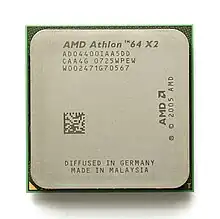
The Athlon 64 X2 is the first native dual-core desktop central processing unit (CPU) designed by Advanced Micro Devices (AMD). It was designed from scratch as native dual-core by using an already multi-CPU enabled Athlon 64, joining it with another functional core on one die, and connecting both via a shared dual-channel memory controller/north bridge and additional control logic. The initial versions are based on the E stepping model of the Athlon 64 and, depending on the model, have either 512 or 1024 KB of L2 cache per core. The Athlon 64 X2 can decode instructions for Streaming SIMD Extensions 3 (SSE3), except those few specific to Intel's architecture. The first Athlon 64 X2 CPUs were released in May 2005, in the same month as Intel's first dual-core processor, the Pentium D.
 Original logo | |
| General information | |
|---|---|
| Launched | May 31, 2005 |
| Discontinued | 2009 |
| Marketed by | AMD |
| Designed by | AMD |
| Common manufacturer(s) |
|
| Performance | |
| Max. CPU clock rate | 1.9 GHz to 3.2 GHz |
| HyperTransport speeds | 1 GHz to 1.8 GHz |
| Architecture and classification | |
| Technology node | 90 nm to 65 nm |
| Microarchitecture | K8 K10 ("Kuma" based models only) |
| Instruction set | MMX, SSE, SSE2, SSE3, x86-64, 3DNow! |
| Physical specifications | |
| Cores |
|
| Socket(s) |
|
| History | |
| Predecessor(s) | Athlon 64 |
| Successor(s) | Phenom |
In June 2007, AMD released low-voltage variants of their low-end 65 nm Athlon 64 X2, named "Athlon X2".[1] The Athlon X2 processors feature reduced thermal design power (TDP) of 45 Watt (W).[2] The name was also used for K10 based budget CPUs with two cores deactivated.
Multithreading
The primary benefit of dual-core processors (like the Athlon 64 X2) over single-core processors is their ability to process more software threads at the same time. The ability of processors to execute multiple threads simultaneously is called thread-level parallelism (TLP). By placing two cores on the same die, the X2 effectively doubles the TLP over a single-core Athlon 64 of the same speed. The need for TLP processing ability depends on the situation to a great degree, and some situations benefit from it far more than others. Some programs are currently written for only one thread, and thus cannot use the processing power of a second core.
Programs often written with multiple threads and able to use dual-cores include many music and video encoding applications, and especially professional rendering programs. High TLP applications currently correspond to server and workstation situations more than the typical desktop. These applications can reach almost twice the performance of a single-core Athlon 64 of the same specifications. Multitasking also runs a sizable number of threads. Intense multitasking processes have sped up by considerably more than twice.[3] This is mostly due to the high overhead caused by constantly switching threads, and could potentially be improved by adjustments to operating system scheduling code.
In the consumer segment of the market, the X2 improves on the performance of the original Athlon 64, especially for multi-threaded software.
Manufacturing costs
Having two cores, the Athlon 64 X2 has an increased number of transistors. The 1 MB L2 cache 90 nm Athlon 64 X2 processor is 219 mm² in size with 243 million transistors [4] whereas its 1 MB L2 cache 90 nm Athlon 64 counterpart is 103.1 mm² and has 164 million transistors.[5] The 65 nm Athlon 64 X2 with only 512 KB L2 per Core reduced this to 118 mm² with 221 million transistors compared to the 65 nm Athlon 64 with 77.2 mm² and 122 million transistors. As a result, a larger area of silicon must be defect free. These size requirements necessitate a more complex fabrication process, which further adds to the production of fewer functional processors per single silicon wafer. This lower yield makes the X2 more expensive to produce than the single-core processor.
In the middle of June 2006 AMD stated that they would no longer make any non-FX Athlon 64 or Athlon 64 X2 models with 1 MB L2 caches.[6] This led to only a small production number of the Socket-AM2 Athlon 64 X2 with 1 MB L2 cache per core, known as 4000+, 4400+, 4800+, and 5200+. The Athlon 64 X2 with 512 KB per core, known as 3800+, 4200+, 4600+, and 5000+, were produced in far greater numbers. The introduction of the F3 stepping then saw several models with 1 MB L2 cache per core as production refinements resulted in an increased yield.
Features
CPU cores
Athlon 64 X2
| AMD Athlon X2 processor family | |||
|---|---|---|---|
| AMD K9 | Desktop | ||
| Code-named | Core | Date released | |
 |
Manchester Toledo Windsor |
dual (90 nm) dual (90 nm) dual (90 nm) |
May 2005 May 2005 May 2006 |
| Toledo Windsor |
dual (90 nm) dual (90 nm) |
Jan 2006 May 2006 | |
 |
Brisbane | dual (65 nm) | Dec 2006 |
| List of AMD Athlon 64 processors List of AMD Athlon X2 processors | |||
Manchester (90 nm SOI)
- Silicon on insulator (SOI)
- CPU stepping: E4
- L1 cache: 64 + 64 KB (data + instructions), per core
- L2 cache: 256, 512 KB full speed, per core
- MMX, Extended 3DNow!, SSE, SSE2, SSE3, AMD64, Cool'n'Quiet, NX Bit
- Socket 939, HyperTransport (1000 MHz, HT1000)
- VCore: 1.35–1.4 V
- Power use (TDP): 89 Watt
- First release: 1 August 2005
- Clock rate: 2000–2400 MHz
- 256 KB L2 cache:
- 3600+: 2000 MHz
- 512 KB L2 cache:
- 3800+: 2000 MHz
- 4200+: 2200 MHz
- 4600+: 2400 MHz (110 Watt TDP)
- 256 KB L2 cache:
Toledo (90 nm SOI)
- Silicon on insulator (SOI)
- CPU stepping: E6
- L1 cache: 64 + 64 KB (data + instructions), per core
- L2 cache: 512 or 1024 KB full speed, per core
- MMX, Extended 3DNow!, SSE, SSE2, SSE3, AMD64, Cool'n'Quiet, NX Bit
- Socket 939, HyperTransport (1000 MHz, HT1000)
- VCore: 1.35–1.4 V
- Power use (TDP):
- 89 Watt: 3800+, 4200+ and 4400+
- 110 Watt: 4400+, 4600+ and 4800+
- First release: 21 April 2005
- Clock rate: 2000–2400 MHz
- 512 KB L2 cache:
- 3800+: 2000 MHz
- 4200+: 2200 MHz
- 4600+: 2400 MHz
- 1024 KB L2 cache:
- 4400+: 2200 MHz
- 4800+: 2400 MHz
- 512 KB L2 cache:
Windsor (90 nm SOI)
%252C_heat_spreader_removed.jpg.webp)
- Silicon on insulator (SOI)
- CPU stepping: F2, F3
- L1 cache: 64 + 64 KB (data + instructions), per core
- L2 cache: 256, 512 or 1024 KB full speed, per core
- MMX, Extended 3DNow!, SSE, SSE2, SSE3, AMD64, Cool'n'Quiet, NX Bit, AMD-V
- Socket AM2, HyperTransport (1000 MHz, HT1000)
- VCore: 1.25–1.35 V
- Power use (TDP):
- 35 Watt (3800+ EE SFF)
- 65 Watt (3600+ to 5200+ EE)
- 89 Watt (3800+ to 6000+)
- 125 Watt (6000+ to 6400+)
- First release: May 23, 2006
- Clock rate: 2000 MHz–3200 MHz
- 256 KB L2 cache:
- 3600+: 2000 MHz
- 512 KB L2 cache: (often mislabeled as Brisbane core)
- 3800+: 2000 MHz
- 4200+: 2200 MHz
- 4600+: 2400 MHz (F2&F3)
- 5000+: 2600 MHz (F2&F3)
- 5400+: 2800 MHz (F3)
- 1024 KB L2 cache:
- 4000+: 2000 MHz
- 4400+: 2200 MHz
- 4800+: 2400 MHz
- 5200+: 2600 MHz (F2&F3)
- 5600+: 2800 MHz (F3)
- 6000+: 3000 MHz (F3)
- 6400+: 3200 MHz (F3)
- 256 KB L2 cache:
Brisbane (65 nm SOI)

- Silicon on insulator (SOI)
- CPU stepping: G1, G2
- L1 cache: 64 + 64 KB (data + instructions), per core
- L2 cache: 512 KB full speed, per core
- MMX, Extended 3DNow!, SSE, SSE2, SSE3, AMD64, Cool'n'Quiet, NX Bit, AMD-V
- Socket AM2, HyperTransport (1000 MHz, HT1000)
- VCore: 1.25–1.35 V
- Die size: 126 mm²
- Power use (TDP): 65 or 89 Watt
- First release: Dec 5, 2006
- Clock rate: 1900 MHz–3100 MHz
- 3600+: 1900 MHz (G1)
- 3800+: 2000 MHz
- 4000+: 2100 MHz
- 4200+: 2200 MHz (G1&G2)
- 4400+: 2300 MHz (G1&G2)
- 4600+: 2400 MHz (G2)
- 4800+: 2500 MHz (G1&G2)
- 5000+: 2600 MHz (G1&G2)
- 5200+: 2700 MHz (G1&G2)
- 5400+: 2800 MHz (G2)
- 5600+: 2900 MHz (G2)
- 5800+: 3000 MHz (G2)
- 6000+: 3100 MHz (G2)
Athlon X2
'64' was omitted from the name of the Brisbane 'BE' series; the 64-bit marketing campaign initiated by AMD became insignificant once essentially all consumer CPUs became 64-bit processors.
Brisbane (65 nm SOI)
- Silicon on insulator (SOI)
- CPU stepping: G2
- L1 cache: 64 + 64 KB (data + instructions), per core
- L2 cache: 512 KB full speed, per core
- MMX, Extended 3DNow!, SSE, SSE2, SSE3, AMD64, Cool'n'Quiet, NX Bit, AMD-V
- Socket AM2, HyperTransport (1000 MHz, HT1000)
- VCore: 1.15–1.20 V
- Die size: 118 mm²
- Power use (TDP): 45 Watt
- First release: October, 2007
- Clock rate: 1900 MHz–2600 MHz
- BE-2300: 1900 MHz (G2)
- BE-2350: 2100 MHz (G2)
- BE-2400: 2300 MHz (G2)
- BE-2450: 2500 MHz (G2)
- 4050e: 2100 MHz (G2)
- 4450e: 2300 MHz (G2)
- 4850e: 2500 MHz (G2)
- 5050e: 2600 MHz (G2)
Kuma (65 nm SOI)
- Chip harvests from Agena with two cores disabled[7]
- Silicon on insulator (SOI)
- AMD K10 microarchitecture
- CPU stepping: B3
- L1 cache: 64 + 64 KB (data + instructions), per core
- L2 cache: 512 KB full speed, per core
- L3 cache: 2 MB (shared)
- MMX, SSE, SSE2, SSE3, SSE4a, Enhanced 3DNow!, NX bit, AMD64, Cool'n'Quiet, AMD-V
- Socket AM2+, HyperTransport (1800 MHz, HT3.0)
- VCore: 1.05–1.25 V
- Die size: 288 mm²
- Power use: (TDP): 95 Watt
- First release: December 15, 2008
- Clock rate: 2300–2800 MHz
- 6500BE: 2300 MHz
- 7450: 2400 MHz
- 7550: 2500 MHz
- 7750BE: 2700 MHz
- 7850BE: 2800 MHz
See also
References
- AMD FAQ on removing the "64" Archived June 10, 2010, at the Wayback Machine
- "DailyTech report". Archived from the original on 2007-06-02. Retrieved 2007-06-04.
- "AMD's dual core Opteron & Athlon 64 X2 - Server/Desktop Performance Preview".
- "Transistors Reference". innoreviews.com. Archived from the original on 2016-11-20. Retrieved 2016-04-29.
- "AMD Athlon™ Processor Model Numbers and Feature Comparison". www.amd.com. Archived from the original on 2009-05-03.
- "HardOCP report". Archived from the original on 2006-06-17. Retrieved 2006-08-08.
- "List of Unlockable AMD CPUs".