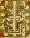
3 µm process
The 3 μm process is the level of MOSFET semiconductor process technology that was reached around 1977,[1][2] by leading semiconductor companies such as Intel.
| Semiconductor device fabrication |
|---|
 |
|
MOSFET scaling (process nodes) |
|
Future
|
Products featuring 3 μm manufacturing process
- Intel's 8085, 8086, 8088 CPU's launched in 1976, 1978, 1979, respectively, were manufactured using its 3.2 μm NMOS (HMOS) process.[1] .[3]
- Hitachi's 4 kbit HM6147 SRAM memory chip, launched in 1978, introduced the twin-well CMOS process, at 3 μm.[4]
- Motorola 68000 (MC68000) CPU, launched in 1979, was originally fabricated using an HMOS process with a 3.5 μm feature size.[5]
- The ARM1 was launched in 1985 and manufactured on a 3 μm process.[6]
References
- Mueller, S (21 July 2006). "Microprocessors from 1971 to the Present". informIT. Retrieved 11 May 2012.
- Myslewski, R (15 November 2011). "Happy 40th birthday, Intel 4004!". TheRegister.
- "History of the Intel Microprocessor - Listoid". Archived from the original on 27 April 2015. Retrieved 5 January 2014.
- "1978: Double-well fast CMOS SRAM (Hitachi)" (PDF). Semiconductor History Museum of Japan. Archived from the original (PDF) on 5 July 2019. Retrieved 5 July 2019.
- Motorola 68000
- "ARM's Race to Embedded World Domination".
| Preceded by 6 μm process |
MOSFET semiconductor device fabrication process | Succeeded by 1.5 μm process |
This article is issued from Wikipedia. The text is licensed under Creative Commons - Attribution - Sharealike. Additional terms may apply for the media files.