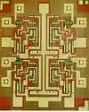
350 nm process
The 350 nanometer process (350 nm process) is a level of semiconductor process technology that was reached in the 1995–1996 timeframe by leading semiconductor companies like Intel and IBM.
| Semiconductor device fabrication |
|---|
 |
|
MOSFET scaling (process nodes) |
|
Future
|
Products featuring 350 nm manufacturing process
- MTI VR4300i (1995), used in the Nintendo 64 game console.
- Intel Pentium (P54CS, 1995), Pentium Pro (1995) and initial Pentium II CPUs (Klamath, 1997).
- AMD K5 (1996) and original AMD K6 (Model 6, 1997) CPUs.
- МЦСТ-R150 (2001).
- Parallax Propeller (2006), 8 core microcontroller.[1]
- Atmel ATmega328, used in the Arduino UNO.[2][3]
References
- "Propeller I semiconductor process technology? Is it 350nm or 180nm?". Parallax Forums. Archived from the original on 2012-07-10. Retrieved 2015-09-13.
- Petryk, Dmytro; Dyka, Zoya (2018). "Optical Fault Injections: a Setup Comparison". S2CID 198917285.
{{cite journal}}: Cite journal requires|journal=(help) - Guillen, Oscar; Gruber, Michael; De Santis, Fabrizio (2017). "Low-Cost Setup for Localized Semi-invasive Optical Fault Injection Attacks: How Low Can We Go?". Constructive Side-Channel Analysis and Secure Design. Lecture Notes in Computer Science. Vol. 10348. pp. 207–222. doi:10.1007/978-3-319-64647-3_13. ISBN 978-3-319-64646-6.
| Preceded by 600 nm |
CMOS manufacturing processes | Succeeded by 250 nm |
This article is issued from Wikipedia. The text is licensed under Creative Commons - Attribution - Sharealike. Additional terms may apply for the media files.