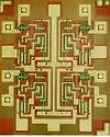
1 µm process
The 1 μm process (1 micrometre process) is a level of MOSFET semiconductor process technology that was commercialized around the 1984–1986 timeframe,[1][2] by leading semiconductor companies like NTT, NEC, Intel and IBM. It was the first process where CMOS was common (as opposed to NMOS).
| Semiconductor device fabrication |
|---|
 |
|
MOSFET scaling (process nodes) |
|
Future
|
The earliest MOSFET with a 1 μm NMOS channel length was fabricated by a research team led by Robert H. Dennard, Hwa-Nien Yu and F.H. Gaensslen at the IBM T.J. Watson Research Center in 1974.[3]
Products featuring 1.0 μm manufacturing process
- NTT introduced the 1 μm process for its DRAM memory chips, including its 64k in 1979 and 256k in 1980.[4]
- NEC's 1 Mbit DRAM memory chip was manufactured with the 1 μm process in 1984.[5]
- Intel 80386 CPU launched in 1985 was manufactured using this process.[1]
- Intel uses this process on the CHMOS III-E technology.[6]
- Intel uses this process on the CHMOS IV technology.[7]
References
- Mueller, S (21 July 2006). "Microprocessors from 1971 to the Present". informIT. Archived from the original on 19 April 2015. Retrieved 11 May 2012.
- Myslewski, R (15 November 2011). "Happy 40th birthday, Intel 4004!". TheRegister. Archived from the original on 19 April 2015. Retrieved 19 April 2015.
- Dennard, Robert H.; Yu, Hwa-Nien; Gaensslen, F. H.; Rideout, V. L.; Bassous, E.; LeBlanc, A. R. (October 1974). "Design of ion-implanted MOSFET's with very small physical dimensions" (PDF). IEEE Journal of Solid-State Circuits. 9 (5): 256–268. Bibcode:1974IJSSC...9..256D. doi:10.1109/JSSC.1974.1050511. S2CID 283984.
- Gealow, Jeffrey Carl (10 August 1990). "Impact of Processing Technology on DRAM Sense Amplifier Design" (PDF). Massachusetts Institute of Technology. pp. 149–166. Retrieved 25 June 2019 – via CORE.
- "Memory". STOL (Semiconductor Technology Online). Retrieved 25 June 2019.
- Intel Corporation, "New Product Focus: Components: Two-and Four-Megabit EPROMs are High-Density Performers", Microcomputer Solutions, September/October 1989, page 14
- Intel Corporation, "New Product Focus: Components: New ASSP Suits Mobile Applications", Microcomputer Solutions, September/October 1990, page 11
External links
| Preceded by 1.5 μm process |
MOSFET semiconductor device fabrication process | Succeeded by 800 nm process |
This article is issued from Wikipedia. The text is licensed under Creative Commons - Attribution - Sharealike. Additional terms may apply for the media files.