Transistor array
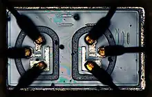
Transistor arrays consist of two or more transistors on a common substrate. Unlike more highly integrated circuits, the transistors can be used individually like discrete transistors. That is, the transistors in the array are not connected to each other to implement a specific function. Transistor arrays can consist of bipolar junction transistors or field-effect transistors. There are three main motivations for combining several transistors on one chip and in one package:[1]
- to save circuit board space and to reduce the board production cost (only one component needs to be populated instead of several)
- to ensure closely matching parameters between the transistors (which is almost guaranteed when the transistors on one chip are manufactured simultaneously and subject to identical manufacturing process variations)
- to ensure a closely matching thermal drift of parameters between the transistors (which is achieved by having the transistors in extremely close proximity)


The matching parameters and thermal drift are crucial for various analogue circuits such as differential amplifiers, current mirrors, and log amplifiers.
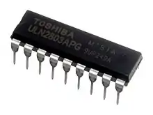
The reduction in circuit board area is particularly significant for digital circuits where several switching transistors are combined in one package. Often the transistors here are Darlington pairs with a common emitter and flyback diodes, e.g. ULN2003A. While this stretches the above definition of a transistor array somewhat, the term is still commonly applied.
A peculiarity of transistor arrays is that the substrate is often available as a separate pin (labelled substrate, bulk, or ground). Care is required when connecting the substrate in order to maintain isolation between the transistors in the array as p–n junction isolation is usually used. For instance, for an array of NPN transistors, the substrate must be connected to the most negative voltage in the circuit.[1]
References
- Dieter Jung (1985-06-30). Transistorarrays [Transistor Arrays] (PDF) (in German). Halbleiterwerk Frankfurt (Oder). OCLC 315025453.