Plasma-activated bonding
Plasma-activated bonding is a derivative, directed to lower processing temperatures for direct bonding with hydrophilic surfaces. The main requirements for lowering temperatures of direct bonding are the use of materials melting at low temperatures and with different coefficients of thermal expansion (CTE).[1]
Surface activation prior to bonding has the typical advantage that no intermediate layer is needed and sufficiently high bonding energy is achieved after annealing at temperatures below 400 °C.
Overview
The decrease of temperature is based on the increase of bonding strength using plasma activation on clean wafer surfaces. Further, the increase is caused by elevation in amount of Si-OH groups, removal of contaminants on the wafer surface, the enhancement of viscous flow of the surface layer and the enhanced diffusivity of water and gas trapped at the interface.[2] Based on ambient pressure, two main surface activation fields using plasma treatment are established for wafer preprocessing to lower the temperatures during annealing.[3] To establish maximum surface energy at low temperatures (< 100 °C) numerous parameters for plasma activation and annealing need to be optimized according to the bond material.[4] Plasma activated bonding is based on process pressure divided into:
- Atmospheric Pressure-Plasma Activated Bonding (AP-PAB)
- Low Pressure-Plasma Activated Bonding (LP-PAB)
- RIE (reactive ion etching)
- ICP RIE (inductively coupled plasma reactive ion etching)
- Sequential plasma (SPAB)
- Remote plasma
Atmospheric Pressure-Plasma Activated Bonding (AP-PAB)
This method is to ignite plasma without using a low pressure environment, so no expensive equipment for vacuum generation is needed.[1]
Atmospheric Pressure-Plasma Activated Bonding enables the possibility to ignite plasma at specific local areas or the whole surface of the substrate. Between the two electrodes plasma gas is ignited via alternating voltage. [3]
The wafer pairs pass the following process flow:
- RCA cleaning
- Surface activation at atmospheric pressure
- Treatment duration ~ 40 s
- Process gases used for silicon
- Synthetic air (80 vol.-% N2 + 20 vol.-% O2)
- Oxygen (O2)
- Process gases used for glass or LiTaO3
- Ar/H2 (90 vol.-% Ar + 10 vol.-% H2)
- Humid oxygen (O2dH2O)
- Rinsing in de-ionized water
- Treatment duration 10 minutes
- Reduction of particle concentration
- Pre-bonding at room temperature
- Annealing (room temperature to 400 °C)
The optimal gas mixture for the plasma treatment is depending on the annealing temperature. Furthermore, treatment with plasma is suitable to prevent bond defects during the annealing procedure.[5]
If using glass, based on the high surface roughness, a chemical-mechanical planarization (CMP) step after rinsing is necessary to improve the bonding quality. The bond strength is characterized by fracture toughness determined by micro chevron tests. Plasma activated wafer bonds can achieve fracture toughnesses that are comparable to bulk material.[3]
Dielectric barrier discharge (DBD)

The usage of dielectric barrier discharge enables a stable plasma at atmospheric pressure. To avoid sparks, a dielectric has to be fixed on one or both electrodes. The shape of the electrode is similar to the substrate geometry used to cover the entire surface. The principle of an AP-activation with one dielectric barrier is shown in figure "Scheme of dielectric barrier discharge".[1]
The activation equipment consists of the grounded chuck acting as wafer carrier and an indium tin oxide (ITO) coated glass electrode. Further, the glass substrate is used as dielectric barrier and the discharge is powered by a corona generator.[2]
Low Pressure-Plasma Activated Bonding (LP-PAB)
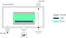
The Low Pressure-Plasma Activated Bonding operates in fine vacuum (0.1 – 100 Pa) with a continuous gas flow. This procedure requires:
- Vacuum
- Process gases
- High frequency (HF) electrical field between two electrodes
The plasma exposed surface is activated by ion bombardment and chemical reactions through radicals. Electrons of the atmosphere move towards the HF electrode during its positive voltage. The most established frequency of the HF electrode is 13.56 MHz.
Further, the electrons are not able to leave the electrode within the positive half wave of applied voltage, so the negative electrode is charged up to 1000 V (bias voltage).[2] The gap between the electrode and the chuck is filled with plasma gas. The moving electrons of the atmosphere are banging into the plasma gas atoms and hit out electrons.[6] Due to its positive orientation the massive ions, that are not able to follow the HF field, move to the negatively charged electrode, where the wafer is placed. Within those environment the surface activation is based on the striking ions and radicals interacting with the surface of the wafer (compare to figure "Scheme of a plasma reactor for low pressure plasma activated bonding").[2]
The surface activation with plasma at low pressure is processed in the following steps:[7]
- RCA cleaning
- Surface activation at low pressure
- Treatment duration ~ 30–60 s
- Process gases (N2, O2)
- Rinsing in de-ionized water
- Treatment duration 10 min
- Reduction of particle concentration
- Pre-bonding at room temperature
- Annealing (room temperature to 400 °C)
Reactive ion etching (RIE)

The RIE mode is used in dry etching processes and through reduction of parameters, i.e. HF power, this method is usable for surface activation.
The electrode attached to the HF-Generator is used as carrier of the wafer. Following, the surfaces of the wafers charge up negatively caused by the electrons and attract the positive ions of the plasma. The plasma ignites in the RIE-reactor (shown in figure "Scheme of a plasma reactor for low pressure plasma activated bonding").
The maximal bond strength is achieved with nitrogen and oxygen as process gases and is sufficiently high with a homogeneous dispersion over the wafers after annealing at 250 °C. The bond energy is characterized > 200 % of non-activated reference wafer annealed at the same temperature. The surface activated wafer pair has 15% less bond energy compared to a high temperature bonded wafer pair. Annealing at 350 °C results in bonding strengths similar to high-temperature bonding.[7]
Remote plasma

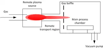
The procedure of remote plasma is based on creating plasma in a separate side chamber. The input gases enter the remote plasma source and are transported to the main process chamber to react. A scheme of the system is shown in figure "Remote plasma system".
Remote plasma is using chemical components where mainly neutral radicals are reacting with the surface. The advantage of this process is less damaged surface through missing ion bombardment. Further, the plasma exposure times could be arranged longer than with, e.g. RIE method.[8]
Sequential plasma (SPAB)
The wafers are activated with short RIE plasma followed by a radical treatment in one reactor chamber. An additional microwave source and an ion trapping metal plate are used for the generation of radicals. The effect of plasma on the surface changes from chemical/physical to chemical plasma treatment. This is based on the reactions between radicals and atoms on the surface.
Technical specifications
| Materials |
|
| Temperature |
|
| Advantages |
|
| Drawbacks |
|
| Researches |
|
References
- D. Wünsch and M. Wiemer and M. Gabriel and T. Gessner (2010). "Low temperature wafer bonding for microsystems using dielectric barrier discharge". MST News. Vol. 1/10. pp. 24–25.
- M. Wiemer and J. Bräuer and D. Wünsch and T. Gessner (2010). "Reactive Bonding and Low Temperature Bonding of Heterogeneous Materials". ECS Transactions. Vol. 33, no. 4. pp. 307–318.
- M. Wiemer and D. Wünsch and J. Bräuer and M. Eichler and P. Hennecke and T. Gessner (2009). "Low temperature bonding of hetero-materials using ambient pressure plasma activation". In R. Knechtel (ed.). WaferBond 2009: Conference on Wafer Bonding for Microsystems 3D- and Wafer Level Integration, Grenoble (France). pp. 73–74.
- M. Eichler and B. Michel and P. Hennecke and C.-P. Klages (2009). "Effects on Silanol Condensation during Low Temperature Silicon Fusion Bonding". Journal of the Electrochemical Society. Vol. 156, no. 10. pp. H786–H793.
- M. Eichler and B. Michel and M. Thomas and M. Gabriel and C.-P. Klages (2008). "Atmospheric-pressure plasma pretreatment for direct bonding of silicon wafers at low temperatures". Surface and Coatings Technology. Vol. 203, no. 5–7. pp. 826–829.
- G. Gerlach and W. Dötzel (March 2008). Ronald Pething (ed.). Introduction to Microsystem Technology: A Guide for Students (Wiley Microsystem and Nanotechnology). Wiley Publishing. ISBN 978-0-470-05861-9.
- D. Wünsch and B. Müller and M. Wiemer and T. Gessner and H. Mischke (2010). "Aktivierung mittels Niederdruckplasma zur Herstellung von Si-Verbunden im Niedertemperatur-Bereich und deren Charakterisierung mittels Mikro-Chevron-Test". Technologien und Werkstoffe der Mikrosystem- und Nanotechnik (GMM-Fachbereicht Band 65). pp. 66–71. ISBN 978-3-8007-3253-1.
- R. E. Belford and S. Sood (2009). "Surface activation using remote plasma for silicon to quartz wafer bonding". Microsystem Technologies. Vol. 15. pp. 407–412. doi:10.1007/s00542-008-0710-4.