Planar process
The planar process is a manufacturing process used in the semiconductor industry to build individual components of a transistor, and in turn, connect those transistors together. It is the primary process by which silicon integrated circuit chips are built, and it is the most commonly used method of producing junctions during the manufacture of semiconductor devices.[1] The process utilizes the surface passivation and thermal oxidation methods.

The planar process was developed at Fairchild Semiconductor in 1959.
The planar process proved to be one of the most important single advances in semiconductor technology.[1]
Overview
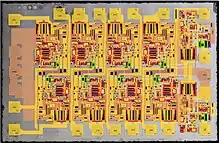
The key concept is to view a circuit in its two-dimensional projection (a plane), thus allowing the use of photographic processing concepts such as film negatives to mask the projection of light exposed chemicals. This allows the use of a series of exposures on a substrate (silicon) to create silicon oxide (insulators) or doped regions (conductors). Together with the use of metallization, and the concepts of p–n junction isolation and surface passivation, it is possible to create circuits on a single silicon crystal slice (a wafer) from a monocrystalline silicon boule.
The process involves the basic procedures of silicon dioxide (SiO2) oxidation, SiO2 etching and heat diffusion. The final steps involves oxidizing the entire wafer with an SiO2 layer, etching contact vias to the transistors, and depositing a covering metal layer over the oxide, thus connecting the transistors without manually wiring them together.
History
Development
At a 1958 Electrochemical Society meeting, Mohamed Atalla presented a paper about the surface passivation of PN junctions by thermal oxidation, based on his 1957 BTL memos.[2]
Swiss engineer Jean Hoerni (one of the "traitorous eight") attended the same 1958 meeting, and was intrigued by Atalla's presentation. Hoerni came up with the "planar idea" one morning while thinking about Atalla's device.[2] Taking advantage of silicon dioxide's passivating effect on the silicon surface, Hoerni proposed to make transistors that were protected by a layer of silicon dioxide.[2] This led to the first successful product implementation of the Atalla silicon transistor passivation technique by thermal oxide.[3]
Jean Hoerni, during his working at Fairchild Semiconductor, had first patented the planar process in 1959.[4][5]
Together with the use of metallization (to join together the integrated circuits), and the concept of p–n junction isolation (from Kurt Lehovec), the researchers at Fairchild were able to create circuits on a single silicon crystal slice (a wafer) from a monocrystalline silicon boule.
In 1959, Robert Noyce built on Hoerni's work with his conception of an integrated circuit (IC), which added a layer of metal to the top of Hoerni's basic structure to connect different components, such as transistors, capacitors, or resistors, located on the same piece of silicon. The planar process provided a powerful way of implementing an integrated circuit that was superior to earlier conceptions of the integrated circuit.[6] Noyce's invention was the first monolithic IC chip.[7][8]
Early versions of the planar process used a photolithography process using near-ultraviolet light from a mercury vapor lamp. As of 2011, small features are typically made with 193 nm "deep" UV lithography.[9] As of 2022, the ASML NXE platform uses 13.5 nm EUV light, generated by a tin-based plasma source.
See also
References
- Butterfield, Andrew J.; Szymanski, John, eds. (2018). A Dictionary of Electronics and Electrical Engineering. Vol. 1. Oxford University Press. doi:10.1093/acref/9780198725725.001.0001. ISBN 978-0-19-872572-5.
- Lojek, Bo (2007). History of Semiconductor Engineering. Springer Science & Business Media. p. 120. ISBN 9783540342588.
- Sah, Chih-Tang (October 1988). "Evolution of the MOS transistor-from conception to VLSI" (PDF). Proceedings of the IEEE. 76 (10): 1280–1326 (1291). Bibcode:1988IEEEP..76.1280S. doi:10.1109/5.16328. ISSN 0018-9219.
- US 3025589 Hoerni, J. A.: "Method of Manufacturing Semiconductor Devices” filed May 1, 1959
- US 3064167 Hoerni, J. A.: "Semiconductor device" filed May 15, 1960
- Bassett, Ross Knox (2007). To the Digital Age: Research Labs, Start-up Companies, and the Rise of MOS Technology. Johns Hopkins University Press. p. 46. ISBN 9780801886393.
- "1959: Practical Monolithic Integrated Circuit Concept Patented". Computer History Museum. Retrieved 13 August 2019.
- "Integrated circuits". NASA. Retrieved 13 August 2019.
- Shannon Hill. "UV Lithography: Taking Extreme Measures". National Institute of Standards and Technology (NIST).
External links
- "The silicon engine: A timeline of semiconductors in computing". Timeline: Browse by decade. Computer history museum. 2012. Retrieved 2012-06-03. A compendium of articles and other information on the development of integrated circuits, including the development of oxide masking, photolithography, the advent of silicon, the integrated circuit and the planar process.
- The Planar Process
- "The history of the integrated circuit". Nobelprize.org. 2003. Retrieved 2012-06-03. An overview of the steps in fabrication of an integrated circuit from the Nobel Prize website. This is a section of the work Techville: The integrated circuit.