1801 series CPU
The 1801 series CPUs were a family of 16-bit Soviet microprocessors based on the indigenous Elektronika NC microarchitecture cores, but binary compatible with DEC's PDP-11 machines. First released in 1980, various models and variants of the series were among the most popular Soviet microprocessors and dominated embedded systems and military applications of the 1980s. They were also used in widely different areas such as graphing calculators (Elektronika MK-85) and industrial CNCs (Elektronika NC series), but arguably their most well-known use was in several Soviet general-purpose mini- and microcomputer designs like the SM EVM, DVK, UKNC, and BK families. Due to being the CPU of the popular Elektronika BK home computer, used in its late years as a demo machine, as well as the DVK micros that often offered a first glimpse into the UNIX world, this processor achieved something of a cult status among Soviet and then Russian programmers, and to a lesser extent, international programmers.
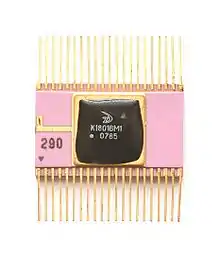 K1801VM1 | |
| General information | |
|---|---|
| Launched | 1980 onwards |
| Common manufacturer(s) | |
| Performance | |
| Max. CPU clock rate | 2 MHz to 12 MHz |
| Architecture and classification | |
| Instruction set | Elektronika NC, LSI-11 |
| Physical specifications | |
| Package(s) | |
Development
The history of this CPU stems from the early 1970s, when the group of engineers in Zelenograd's Special Computing Center, led by D.I. Yuditsky, developed their first 16-bit minicomputer, called Elektronika NC-1. This machine, intended to directly compete with SM EVM series, was first released in 1973 and used the bit slice 4-bit 587 CPU, sometimes called the first Soviet microprocessor ever. Its descendants proved popular and were widely used in various control systems and telecom equipment. However, the bit-slice nature of their CPUs made these machines somewhat unwieldy, especially in military applications, and the need for a single-chip microprocessor was identified.
In 1980 the first 1801 CPU intended to fill this niche, K1801VE1, entered production. It was essentially a microcontroller with 256 bytes of on-chip RAM, 2K ROM and other peripheral circuitry, still based on Elektronika NC instruction set, but compatible with a Soviet clone of DEC's Q-Bus that was already adopted as an industry standard — a first sign of things to come. Its peripheral circuits were underutilized by the industry, as it was mostly used as a general-purpose CPU, rather than a microcontroller, so it was decided to simplify the chip, removing unnecessary devices from the die. But by that time its parent organization, the SCC, has already lost in the power games that plagued Soviet industry.
By its nature, Soviet industry was an extremely bureaucratic structure, so decision making process was often driven not by technical or economical considerations, but by the results of the games of influence between various organizations and officials. SCC, despite its technical successes and popularity of its designs, was not without its opponents and even enemies. While its staff had an aversion to copying and reverse engineering Western technology, many groups within the Ministry of Electronic Industry argued for it as a quicker and more secure way to meet the needs. These groups eventually prevailed, and in 1976 the SCC was essentially disbanded, its technical base passing to the Angstrem plant while some of its research labs were joined to the Research Institute of Precision Technology (which didn't really need them), and others forming a research arm of the newly formed NPO Scientific Center.
Discontinuation
This sudden reorganization resulted in the abandonment of the Elektronika NC architecture (it continued only in CNCs based on an NC-1 machine, some of which are used up to this day) and the adoption of the PDP-11 compatibility as a MEI standard, a process sometimes called PDP revolt in Russian literature. Thus, the microcode for the new simplified CPU was redesigned and made compatible with LSI-11 instruction set. The new processor was released in 1982, designated K1801VM1. It was supplemented by the 600-gate KR1801VP1 (Russian: КР1801ВП1) gate array, which was used to implement various support circuitry, 64 Kib KR1801RE2 ROM chip, and 64 Kib K573RF3 EPROM. Together they constituted the first widely used generation of 1801 family. The KR18101VP1 gate array was later manufactured by a number of second sources: Exiton Pavlovsky Posad, SEMZ Solnechnogorsk, and Intermos in Hungary.[1]
Technical characteristics
All CPUs in the family were single-chip 16-bit microprocessors based on Elektronika NC microarchitecture, however only the first one, the K1801VE1 microcontroller, used the Electronica NC instruction set. Others have an updated microcode implementing the LSI-11 architecture. Various models differed in clock speed, instruction set (the first models lacked the MUL and DIV commands, for example), package and address bus width (the latest models supported 22-bit addressing). In terms of raw processing power, it is roughly comparable to US-made Intel 286.
K1801VE1
K1801VM1
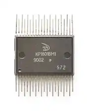
- Instruction set: LSI-11; supported EIS instructions:
XOR,SOB,MUL(MUL only in the rare 1801VM1G variant) - Technology: 5 μm nMOS
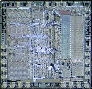
- Die size: 5x5 mm, 16646 transistors[2]
- Bus: МПИ (Q-Bus, multiplexed)
- Clock speed: 100 kHz — 5 MHz
- Voltage: +5 V
- Power: 1.2 W
- Package: 42-pin ceramic planar (K1801VM1, image above) or plastic planar (KR1801VM1)
- Variants:[3]: 202–206 [1]
- A (А) — max. clock frequency 5 MHz (often marked with one dot on the package)
- B (Б) — max. clock frequency 4 MHz
- V (В) — max. clock frequency 3 MHz
- G (Г) — max. clock frequency 5 MHz;
MULinstruction is supported (often marked with two dots on the package)
- Second source: Exiton Pavlovsky Posad
K1801VM2
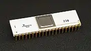
- Instruction set: LSI-11 (
MUL/DIVincluded, FIS codes implemented by ROM interrupt routines)[4] - Technology: 4 μm nMOS (a later CMOS version was designated 1806VM2)
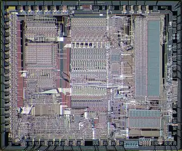
- Die size: 5.3x5.35 mm, 18500 transistors[5]
- Bus: МПИ (Q-Bus, multiplexed)
- Clock speed: 2 — 10 MHz
- Voltage: +5 V
- Power: 1.7 W
- Package: 40-pin CERDIP (KM1801VM2) or PDIP (KR1801VM2, military variant R1802VM2)
- Second source: SEMZ Solnechnogorsk
It has two different address spaces and the ability to quickly switch between them. They were used in implementing the FIS instruction subset, with instructions processed not in microcode, but as interrupt handlers in shadow ROM.

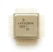
K1801VM3
- Instruction set: LSI-11; EIS and MMU (
MTPD,MTPI,MFPD,MFPI) included - Technology: 4 μm nMOS (later CMOS versions were designated 1806VM3U, 1806VM5U and N1836VM3)
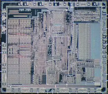
- Die size: 6.65x8 mm, 28900 transistors[6]
- Bus: МПИ (Q-Bus, multiplexed)
- Clock speed: 4 — 6 MHz, and 8 MHz from 1991
- Voltage: +5 V
- Power: 1.7 W
- Package: 64-pin CERDIP (KM1801VM3) or 64-pin CQFP (N1801VM3)
- Address bus: 22-bit
- Supports floating point coprocessor[7]
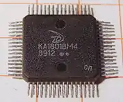
K1801VM4
- Floating point coprocessor for K1801VM3, 32/64 bit, clocked at 6 MHz (8 MHz after 1991)
- Technology: nMOS (later CMOS versions were designated 1806VM4U and N1836VM4)
- DEC PDP-11 FPU instructions LDUB, LDSC, STA0, STB0 and STQ0 have not been implemented.
- Package: 64-pin plastic planar (KA1801VM4) or 64-pin CQFP (KN1801VM4)
Further development
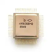
1806 series
- All devices in the 1806 series are manufactured in CMOS technology and require a +5 V power supply.
- 1806VM2: functionally equivalent to the nMOS K1801VM2; clock speed 5 MHz; 42-pin ceramic planar package; 134636 transistors[8][9][10][11]
- N1806VM2: functionally equivalent to the nMOS K1801VM2; clock speed 5 MHz; 64-pin CQFP; 134636 transistors; manufactured by Fizika Moscow as a second source[8][9][10][11]
- 1806VM3U: functionally equivalent to the nMOS K1801VM3; clock speed 8 MHz; 64-pin CQFP[10]
- 1806VM4U: functionally equivalent to the nMOS K1801VM4; clock speed 8 MHz; 64-pin CQFP[10]
- 1806VM5U: functionally equivalent to the nMOS K1801VM3; clock speed 16 MHz; 64-pin CQFP[10]
- Similar to the 1801VP1 for the 1801 series, peripheral functions for the 1806 series are implemented using the gate arrays 1806VP1 (Russian: 1806ВП1), 1806KhM1 (Russian: 1806ХМ1, later renamed to 1806BTs1, Russian: 1806БЦ1),[8] and 1582VZh3 (Russian: 1582ВЖ3).[9]
KA1013VM1
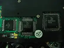
- Technology: CMOS[12]
- Clock speed: — 2 MHz
- Voltage: +4.5 ... +6 V
- Microcontroller. It uses an 1806VM2 core with support logic implemented in ULAs placed on the same die. Includes keyboard controller, UART, parallel interface, MMU, watchdog timer and PMU. Memory is external. The development version was called T36VM1-2.
1836 series
- All devices in the 1836 series are manufactured in CMOS technology and require a +5 V power supply. They are manufactured by Fizika Moscow as a second source.
- N1836VM3: functionally equivalent to the nMOS K1801VM3; clock speed 25 MHz; 64-pin CQFP[1][9][13]
- N1836VM4: functionally equivalent to the nMOS K1801VM4; clock speed 16 MHz; 64-pin CQFP[9][13]
- Die photos
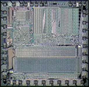 K1801VM1
 KM1801VM2
 KM1801VM3
 N1806VM2
Use
These CPUs were used in:
- Soyuz-Neon PC-11/16 PC, roughly similar to AT in performance (N1806VM2)
- DVK series professional micro computers (various)[4][7]
- UKNC educational computers (KM1801VM2)
- BK home computers (KM1801VM1)
- BASIC-programmable calculator "Elektronika MK-85" (Russian: Электроника МК-85; based on KA1013VM1)
- Elektronika NC-31 lathe-control CNC
- Elektronika IM-05 chess computer (1801VM2)[4]
- "Romashka" electronic typewriter (1801VM2)[4]
- Buran space shuttle (1806 series)[14]
- Various military and industrial applications
- Hungarian computers SZAMALK Mikrosztar 1123, MTA KFKI TPA-11/30 (both K1801VM2)[15]
References
- "1801ая серия" [1801 Series] (in Russian). Retrieved 11 July 2016.
- "Цифровая археология: 1801 и все-все-все" [Digital archeology: 1801 and all-all] (in Russian). Retrieved 16 January 2019.
- Ниссельсон, Л.И. (1989). Цифровые и аналоговые интегральные микросхемы [Digital and analog integrated circuits] (in Russian). Радио и связь. ISBN 5256002597.
- "The Soviet 1801VM2 LSI-11 Processor". cpushack.com. 4 November 2021. Retrieved 8 December 2022.
- "Цифровая археология: 1801 и все-все-все" [Digital archeology: 1801 and all-all] (in Russian). Retrieved 16 January 2019.
- "Цифровая археология: 1801 и все-все-все" [Digital archeology: 1801 and all-all] (in Russian). Retrieved 16 January 2019.
- "The Soviet 1801VM3 Enhanced LSI-11 Processor". cpushack.com. 20 November 2021. Retrieved 8 December 2022.
- "1806ая серия" [1806 Series] (in Russian). Retrieved 11 July 2016.
- "Компоненты микропроцессорных систем" [Components for microprocessor systems] (in Russian). Moscow: NPO Fizika. Retrieved 22 November 2016.
- "Integrated circuits (IC) for computing devices". Zelenograd: Techno unity. Retrieved 25 November 2016.
- "16-разрядный LSI/2-совместимый микропроцессор" [16-bit LSI/2-compatible microprocessor] (in Russian). Zelenograd: Angstrem. Archived from the original on 15 May 2016. Retrieved 22 November 2016.
- Нефедов, А.В. (2000). Интегральные микросхемы и их зарубежные аналоги. Том 07. Серии К700-К1043 [Integrated circuits and their foreign equivalents. Volume 07. Series K700-K1043.] (in Russian). Moscow: ИП РадиоСофт. ISBN 5-93037-003-6. Retrieved 21 October 2016.
- "16-разрядный LSI-11/23-совместимый комплект" [16-bit LSI-11/23-compatible series] (in Russian). Zelenograd: Angstrem. Archived from the original on 15 May 2016. Retrieved 22 November 2016.
- "Russian Computers on the Buran Shuttle". CPU Shack. 20 February 2011. Retrieved 24 November 2016.
- "SCIENCE & TECHNOLOGY - EUROPE & LATIN AMERICA" (PDF). Defense Technical Information Center. 22 June 1987. pp. 66–75. Archived from the original on August 25, 2016. Retrieved 12 February 2018.
External links
- 1801BM1 (15 January 2023). "Revengineered ancient PDP-11 CPUs, originals and clones". GitHub.