< Nanotechnology
| Navigate |
|---|
| << Prev: Background Material |
| >< Main: Nanotechnology |
| >> Next: Overview of Production Methods |
|
|
| <<< Prev Part: Physics - on the nanoscale |
| >>> Next Part: Nanosystems |
This part will give an overview of nanomaterials - the production methods, their properties, brief examples of applications and demonstrations of their capabilities.
Apart from a general overview of production methods, we have divided the materials as
- Semiconducting
- Metallic
- Organic
A division that might be up for revision shortly.
|
One way to classify a material is its electronic structure 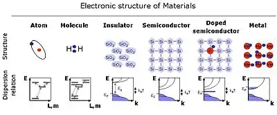
Overview of the electronic structure of the different fundamental classes of materials.
Atoms have discrete energy levels for each electronic state. Electronic transitions by eg. optical excitation can change the state of the atom.
Molecules can also have discrete energy levels, but the more complex structure also gives a much more complex diagram of electronic states. In addition, the molecules con rotate and vibrate which modulates the oberserved energy levels.
Insulators can be seen as a condensed phase of molecules with little electronic connection between neighboring molecules for conducting a current. Only when excitation is made with an energy above the several eV bandgap will conduction be possible.
Semiconductors have a more narrow bandgap and even at room temperature a few conduction electrons will be excited into the conductance band.
Doped Semiconductors have higher electrical conductance because added dopants provide conduction electrons.
Metals can be considered as ionized metal atoms in a sea of free electrons, giving a high conductivity and high reflectivity of light (as long as it is not too high in frequency).
|
Another is according to their geometry  overview of nanoscale structure geometries |
Overview of nanomaterials
| Type | Structure | Production | Properties | |
|---|---|---|---|---|
| Buckyballs/ C60 | 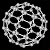 Buckminsterfullerene C60 -60 Carbon atoms arranged as in football |
|||
| Single Wall Carbon Nanotubes (SWCNT) | 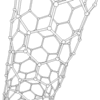 This animation of a rotating Carbon nanotube shows its 3D structure. A single shell of carbon atoms arranged in a cylindrical chicken-wire-like hexagonal structure with diameter from about 2 nm. |
Semiconducting or metallic depending on how the carbon lattice is twisted. | ||
| Multi Wall Carbon Nanotubes (MWCNT) | Concentric shells of SWCNT, diameter up to hundreds of nm | |||
| Silicon Nanowires and heterostructures | Silicon crystals with diameters from a few nm | Typically VLS growth | ||
| III-V Nanowires | crystals with diameters from a few nm | typically VLS growth. A wealth of heterostructures can be formed to make tunnel barrier junctions etc. | Semiconducting, often optically active and fluorescing due to direct bandgap (unlike silicon). | |
| Gold nanoparticles | ||||
| Silica nanoparticles | ||||
| Platinum nanoparticles | small metallic clusters | Used as catalysts in many reactions |
Further reading
References
See also notes on editing this book about how to add references Nanotechnology/About#How_to_contribute.
This article is issued from Wikibooks. The text is licensed under Creative Commons - Attribution - Sharealike. Additional terms may apply for the media files.