< Microtechnology 
Materials
Overview

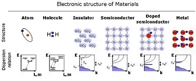
Overview of the electronic structure of the different fundamental classes of materials.
Atoms have discrete energy levels for each electronic state. Electronic transitions by eg. optical excitation can change the state of the atom.
Molecules can also have discrete energy levels, but the more complex structure also gives a much more complex diagram of electronic states. In addition, the molecules can rotate and vibrate which modulates the observed energy levels.
Insulators can be seen as a condensed phase of molecules with little electronic connection between neighboring molecules for conducting a current. Only when excitation is made with an energy above the several eV bandgap will conduction be possible.
Semiconductors have a more narrow bandgap and even at room temperature a few conduction electrons will be excited into the conductance band.
Doped Semiconductors have higher electrical conductance because added dopants provide conduction electrons.
Metals can be considered as ionized metal atoms in a sea of free electrons, giving a high conductivity and high reflectivity of light (as long as it is not too high in frequency)
Resources with overviews of materials and their most prominent uses:
- Semiconductor materials
- Ioffe NSM data archive
- overview of microfabrication materials
- overview of microfabrication materials
- Semiconductor materials
- polymers
Overview table of microfabrication materials
| Material | Typical use | Density [g/cm3] | Atm. Mass[g/mol] | Youngs Modulus[GPa] | Shear modulus [GPa] | El. Conductivity | Therm. Cond.[W·m−1·K−1] | Melting point[K] | Notes |
|---|---|---|---|---|---|---|---|---|---|
| Aluminium | Leads | 2.70 | 26.98 | 70 | 26 | 26.50 nΩ·m | 237 | 933.47 K (660.32 °C) | Add notes |
| Gallium Arsenide | Light emitter | 5.3176 | 144.645 | youngs | bulk | el. | therm. | 1238°C (1511 K) | Bandgap 1.424 eV |
| Gallium Nitride | Blue Light emitter | 6.1 | 83.7297 | youngs | bulk | el. | therm. | K ( °C) | Add notes |
| Polysilicon | solar cells | den | amu | youngs | bulk | el. | therm. | K ( °C) | highly dependent on doping and annealing. Se detailed table in the silicon section |
| Silicon | Wafers, semiconductor | 2.33 | 28.0855(3) | 47 | bulk | el. | 149 | 1687 K (1414 °C) | highly dependent on doping. Se detailed table in the silicon section |
| Silicon dioxide, silica | insulator, light waveguide | den | amu | youngs | bulk | el. | therm. | K ( °C) | Add notes |
| Silicon nitride | insulator | den | amu | youngs | bulk | el. | therm. | K ( °C) | Add notes |
| Gold | Coating of leads | 19.3 | 196.966569 | 78 | 220 | 22.14 nΩ·m | 318 | 1337.33 K (1064.18 °C) | Add notes |
| Nickel | MEMS, leads | den | amu | youngs | bulk | el. | therm. | K ( °C) | Add notes |
| Platinum | Contact pads | den | amu | youngs | bulk | el. | therm. | K ( °C) | Add notes |
| PMMA | 1.19 | 50.000-950.000 | youngs | bulk | el. | therm. | 378 K (105°C) glass trans. | Refractive index 1.492 | |
| SU8 polymer | den | amu | youngs | bulk | el. | therm. | K ( °C) | Add notes | |
| Tungsten | den | amu | youngs | bulk | el. | therm. | K ( °C) | Add notes |
This table should be merged with the above...
| Mechanical | Thermal | Electrical | ||||||||
| Yield Str. | Youngs. | Pois. | Density | Th. Cond. | Th. Exp. | Melting | El. cond. | α | ||
| Highest Z | Material | GPa | GPa | ? | kg/m³ | (W/cmK) | (ppm/K) | K | Ωm | promille/K |
| Metals | ||||||||||
| 34 | Al | 0.17 | 70 | 0.34 | 2698 | 2.36 | 23 | 660 | 26.5*10?? | 4.3 |
| 55 | Au | ? | 78-80 | 0.44-0.25 | 19281 | 3.12 | 14 | 1064 | 23-22.1*10?? | 3.7 |
| 66 | Cr | ? | ? | ? | 7194 | ? | ? | 1860 | ? | |
| 55 | Ti | 0.23 | 116 | 0.32 | 4508 | 0.2 | 8.5 | 1670 | 420*10?? | 3.8 |
| 80 | Pt | 0.12 | 168 | 0.38 | 21450 | 0.73 | 8.9 | 1772 | 0.0981? | 3.9 |
| 78 | W | 0.12 | 411 | 0.28 | 19254 | 1.8 | 4.5 | 3387 | 0.0489? | 4.8 |
| 65 | Ag | ? | ? | ? | ? | ? | ? | 960 | 15.9*10?? | |
| 56 | Fe | 12.6 | 196 | 0.29 | 7873 | 0.803 | 11.7-12 | 1540 | 89E | 6.6 |
| Semimetals | ||||||||||
| 12 | Graphite | ? | ? | ? | 2266 | ? | ? | 3700 | 7-60E | -0.4 |
| Semiconductors | ||||||||||
| 25 | Si intrinsic | 7 | 190 | ? | 2329 | 1.57 | 2.33 | 1410 | 2.5*10³ | |
| 25 | poly Si | ? | 150-170 | 0.3-0.066 | 2320 | 0.5-0.34 | 2.6 | ? | 22000 | |
| 25 | SiC | 21 | 700 | ? | 3200 | 3.5 | 3.3 | ? | ? | |
| 45 | InP | ? | 7.1E11 dyn cm-2 | ? | 4810 | 0.68 W cm-1 °C-1 | 4.60·10-6 °C-1 | 1060 | ? | |
| Insulators | ||||||||||
| 12 | Diamond | 53 | 1035 | ? | 3500 | 20 | 1 | ? | 2.7 | |
| 34 | Al2O3 | 15.4 | 530 | ? | 4000 | 0.5 | 5.4 | ? | ? | |
| 25 | SiO2 (bulk) | 8.4 | 73 | ? | 25-2150 | 0.014 | 0.55 | ? | E-12 | |
Units
- 1 g/cm3 = 1 kg/L = 1000 kg/m3
- g/mol = amu = Da
Applications and Uses
- Microprocessors
- Transistors
- Lab-on-a-chip
- MEMS
Product Life-Cycles
Cheap and disposable point-of-care microfluidic chips require very different materials compared to high performance microprocessors.
Environmental Considerations
The environmental footprint of microfabriaction is not discussed very often. If anyone has knowledge about this I hope they will contribute!!
Wafers and Substrates
Overview of wafer types, flats, cleaving planes etc.
References
See also notes on editing this book about how to add references Microtechnology/About#How to Contribute.
This article is issued from Wikibooks. The text is licensed under Creative Commons - Attribution - Sharealike. Additional terms may apply for the media files.