Walter Houser Brattain
Walter Houser Brattain (/ˈbrætən/; February 10, 1902 – October 13, 1987) was an American physicist at Bell Labs who, along with fellow scientists John Bardeen and William Shockley, invented the point-contact transistor in December 1947.[1] They shared the 1956 Nobel Prize in Physics for their invention. Brattain devoted much of his life to research on surface states.
Walter Houser Brattain | |
|---|---|
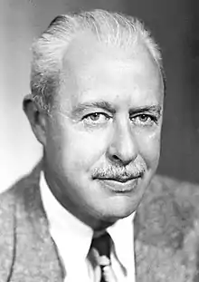
 Brattain c. 1950 | |
| Born | February 10, 1902 Xiamen, Fujian, China |
| Died | October 13, 1987 (aged 85) Seattle, Washington, U.S. |
| Nationality | American |
| Alma mater | |
| Known for | Transistor |
| Relatives | Robert Brattain (brother) |
| Awards |
|
| Scientific career | |
| Fields | Physics, electronic engineering |
| Institutions | |
| Doctoral advisor | John Torrence Tate Sr. |
Biography
Walter Brattain was born in Amoy (now Xiamen), Fujian, Qing China, to American parents Ross R. Brattain and Ottilie Houser Brattain.[2] Ross R. Brattain was a teacher at the Ting-Wen Institute,[3]: 11 a private school for Chinese boys; Ottilie Houser Brattain was a gifted mathematician.[4] Both were graduates of Whitman College.[5]: 71 [6] Ottilie and baby Walter returned to the United States in 1903, and Ross followed shortly afterward.[3]: 12 The family lived for several years in Spokane, Washington, then settled on a cattle ranch near Tonasket, Washington in 1911.[3]: 12 [5]: 71
Brattain attended high school in Washington, spending one year at Queen Anne High School in Seattle, two years at Tonasket High School, and one year at Moran School for Boys on Bainbridge Island.[7] Brattain then attended Whitman College in Walla Walla, Washington, where he studied with Benjamin H. Brown (physics) and Walter A. Bratton (mathematics). He earned a bachelor's degree from Whitman in 1924, with a double major in physics and mathematics.[8] Brattain and his classmates Walker Bleakney, Vladimir Rojansky and E. John Workman would all go on to have distinguished careers, later becoming known as "the four horsemen of physics".[5]: 71 Brattain's brother Robert, who followed him at Whitman College, also became a physicist.[5]: 71
Brattain earned a Master of Arts from the University of Oregon in Eugene in 1926, and a Ph.D. from the University of Minnesota in 1929.[8][9] At Minnesota, Brattain had the opportunity to study the new field of quantum mechanics under John Hasbrouck Van Vleck. His thesis, supervised by John T. Tate, was Efficiency of Excitation by Electron Impact and Anomalous Scattering in Mercury Vapor.[5]: 72
Walter Brattain married twice. His first wife was chemist Keren Gilmore. They were married in 1935 and had a son, William G. Brattain, in 1943. Keren Gilmore Brattain died on April 10, 1957.[10] The following year, Brattain married Mrs. Emma Jane (Kirsch) Miller, a mother of three children.[8]
He moved to Seattle in the 1970s and lived there until his death from Alzheimer's disease on October 13, 1987.[2][9] He is buried at City Cemetery in Pomeroy, Washington.
Scientific work
From 1927 to 1928 Brattain worked for the National Bureau of Standards in Washington, D.C., where he helped to develop piezoelectric frequency standards. In August 1929 he joined Joseph A. Becker at Bell Telephone Laboratories as a research physicist.[11] The two men worked on the heat-induced flow of charge carriers in copper oxide rectifiers.[5]: 72 Brattain was able to attend a lecture by Arnold Sommerfeld.[11] Some of their subsequent experiments on thermionic emission provided experimental validation for the Sommerfeld theory. They also did work on the surface state and work function of tungsten and the adsorption of thorium atoms.[5]: 74 Through his studies of rectification and photo-effects on the semiconductor surfaces of cuprous oxide and silicon, Brattain discovered the photo-effect at the free surface of a semiconductor. This work was considered by the Nobel prize committee to be one of his chief contributions to solid state physics.[2]
At the time, the telephone industry was heavily dependent on the use of vacuum tubes to control electron flow and amplify current. Vacuum tubes were neither reliable nor efficient, and Bell Laboratories wanted to develop an alternative technology.[12] As early as the 1930s Brattain worked with William B. Shockley on the idea of a semiconductor amplifier that used copper oxide, an early and unsuccessful attempt at creating a field effect transistor. Other researchers at Bell and elsewhere were also experimenting with semiconductors, using materials such as germanium and silicon, but the pre-war research effort was somewhat haphazard and lacked strong theoretical grounding.[13]
During World War II, both Brattain and Shockley were separately involved in research on magnetic detection of submarines with the National Defense Research Committee at Columbia University.[8] Brattain's group developed magnetometers sensitive enough to detect anomalies in the Earth's magnetic field caused by submarines.[3]: 104 [11] As a result of this work, in 1944, Brattain patented a design for a magnetometer head.[14]
In 1945, Bell Labs reorganized and created a group specifically to do fundamental research in solid state physics, relating to communications technologies. Creation of the sub-department was authorized by the vice-president for research, Mervin Kelly.[13] An interdisciplinary group, it was co-led by Shockley and Stanley O. Morgan.[5]: 76 The new group was soon joined by John Bardeen.[13] Bardeen was a close friend of Brattain's brother Robert, who had introduced John and Walter in the 1930s.[3] They often played bridge and golf together.[5]: 77 Bardeen was a quantum physicist, Brattain a gifted experimenter in materials science, and Shockley, the leader of their team, was an expert in solid-state physics.[15]


According to theories of the time, Shockley's field effect transistor, a cylinder coated thinly with silicon and mounted close to a metal plate, should have worked. He ordered Brattain and Bardeen to find out why it wouldn't. During November and December the two men carried out a variety of experiments, attempting to determine why Shockley's device wouldn't amplify.[12] Bardeen was a brilliant theorist;[16] Brattain, equally importantly, "had an intuitive feel for what you could do in semiconductors".[13]: 40 Bardeen theorized that the failure to conduct might be the result of local variations in the surface state which trapped the charge carriers.[17]: 467–468 Brattain and Bardeen eventually managed to create a small level of amplification by pushing a gold metal point into the silicon, and surrounding it with distilled water. Replacing silicon with germanium enhanced the amplification, but only for low frequency currents.[12]
On December 16, Brattain devised a method of placing two gold leaf contacts close together on a germanium surface.[15] Brattain reported: "Using this double point contact, contact was made to a germanium surface that had been anodized to 90 volts, electrolyte washed off in H2O and then had some gold spots evaporated on it. The gold contacts were pressed down on the bare surface. Both gold contacts to the surface rectified nicely... One point was used as a grid and the other point as a plate. The bias (D.C.) on the grid had to be positive to get amplification"[17]
As described by Bardeen, "The initial experiments with the gold spot suggested immediately that holes were being introduced into the germanium block, increasing the concentration of holes near the surface. The names emitter and collector were chosen to describe this phenomenon. The only question was how the charge of the added holes was compensated. Our first thought was that the charge was compensated by surface states. Shockley later suggested that the charge was compensated by electrons in the bulk and suggested the junction transistor geometry... Later experiments carried out by Brattain and me showed that very likely both occur in the point-contact transistor."[17]: 470
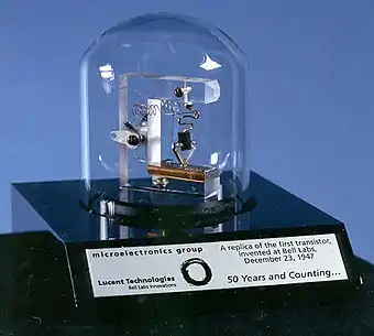
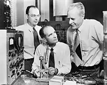
On December 23, 1947, Walter Brattain, John Bardeen, and William B. Shockley demonstrated the first working transistor to their colleagues at Bell Laboratories. Amplifying small electrical signals and supporting the processing of digital information, the transistor is "the key enabler of modern electronics".[18] The three men received the Nobel Prize in Physics in 1956 "for research on semiconductors and the discovery of the transistor effect."[8]
Convinced by the 1947 demonstration that a major breakthrough was being made, Bell Laboratories focused intensively on what it now called the Surface States Project. Initially, strict secrecy was observed. Carefully restricted internal conferences within Bell Labs shared information about the work of Brattain, Bardeen, Shockley and others who were engaged in related research.[17]: 471 Patents were registered, recording the invention of the point-contact transistor by Bardeen and Brattain.[19] There was considerable anxiety over whether Ralph Bray and Seymour Benzer, studying resistance in germanium at Purdue University, might make a similar discovery and publish before Bell Laboratories.[13]: 38–39
On June 30, 1948, Bell Laboratories held a press conference to publicly announce their discovery. They also adopted an open policy in which new knowledge was freely shared with other institutions. By doing so, they avoided classification of the work as a military secret, and made possible widespread research and development of transistor technology. Bell Laboratories organized several symposia, open to university, industry and military participants, which were attended by hundreds of scientists in September 1951, April 1952, and 1956. Representatives from international as well as domestic companies attended.[17]: 471–472, 475–476
Shockley believed (and stated) that he should have received all the credit for the discovery of the transistor.[19][20][21] He actively excluded Bardeen and Brattain from new areas of research,[22] in particular the junction transistor, which Shockley patented.[19] Shockley's theory of the junction transistor was an "impressive achievement", pointing the way to future solid-state electronics, but it would be several years before its construction would become practically possible.[13]: 43–44
Brattain transferred to another research group within Bell Laboratories, working with C. G. B. Garrett, and P. J. Boddy. He continued to study the surface properties of solids and the "transistor effect", so as to better understand the various factors underlying semiconductor behavior.[5]: 79–81 [23] Describing it as "an intolerable situation", Bardeen left Bell Laboratories in 1951 to go to the University of Illinois, where he eventually won a second Nobel Prize for his theory of superconductivity.[19] Shockley left Bell Laboratories in 1953 and went on to form the Shockley Semiconductor Laboratory at Beckman Instruments.[22][24]
In 1956, the three men were jointly awarded the Nobel Prize in Physics by King Gustaf VI Adolf of Sweden "for research on semiconductors and the discovery of the transistor effect."[8] Bardeen and Brattain were included for the discovery of the point-contact transistor; Shockley for the development of the junction transistor. Walter Brattain is credited as having said, when told of the award, "I certainly appreciate the honor. It is a great satisfaction to have done something in life and to have been recognized for it in this way. However, much of my good fortune comes from being in the right place, at the right time, and having the right sort of people to work with."[25] Each of the three gave a lecture. Brattain spoke on Surface Properties of Semiconductors,[26] Bardeen on Semiconductor Research Leading to the Point Contact Transistor,[27] and Shockley on Transistor Technology Evokes New Physics.[28]
Brattain later collaborated with P. J. Boddy and P. N. Sawyer on several papers on electrochemical processes in living matter.[5]: 80 He became interested in blood clotting after his son required heart surgery. He also collaborated with Whitman chemistry professor David Frasco, using phospholipid bilayers as a model to study the surface of living cells and their absorption processes.[22]
Teaching
Brattain taught at Harvard University as a visiting lecturer in 1952 and at Whitman College as a visiting lecturer in 1962 and 1963, and a visiting professor beginning in 1963. Upon formally retiring from Bell Laboratories in 1967, he continued to teach at Whitman, becoming an adjunct professor in 1972. He retired from teaching in 1976 but continued to be a consultant at Whitman.[8]
At Whitman, the Walter Brattain Scholarships are awarded on a merit basis to "entering students who have achieved high academic excellence in their college preparatory work." All applicants for admission are considered for the scholarship, which is potentially renewable for four years.[29]
Awards and honors
Walter Brattain has been widely recognized for his contributions.[8]
- Awards
- Stuart Ballantine Medal of the Franklin Institute, 1952 (jointly with Dr. John Bardeen)[30]
- John Scott Medal, 1954 (jointly with Dr. John Bardeen)
- Nobel Prize in Physics, 1956 (jointly with Dr. John Bardeen and Dr. William B. Shockley)[25]
- Inducted into the National Inventors Hall of Fame, 1974
- Memberships
- Honorary degrees
- Doctor of Science, Portland University, 1952
- Whitman College, 1955
- Union College, 1955 (jointly with Dr. John Bardeen)
- University of Minnesota, 1957
- Other recognition
- USS Brattain, Star Trek: The Next Generation, "Night Terrors"
References
- "Walter H. Brattain". IEEE Global History Network. IEEE. Retrieved August 10, 2011.
- "Walter Houser Brattain". Royal Swedish Academy of Sciences. Retrieved December 8, 2014.
Walter H. Brattain was born in Amoy, China, on February 10, 1902, the son of Ross R. Brattain and Ottilie Houser. ...
- Riordan, Michael; Hoddeson, Lillian (1998). Crystal fire : the invention of the transistor and the birth of the information age. New York [u.a.]: Norton. p. 78. ISBN 9780393318517. Retrieved March 4, 2015.
- Cooper, David Y. (2001). "Brattain, Walter H. (1902–1987), Physicists, Physicists, Nobel Prize Winners". American National Biography Online. doi:10.1093/anb/9780198606697.article.1301949. ISBN 9780198606697. Retrieved March 4, 2015.
- Bardeen, John (1994). Walter Houser Brattain 1902–1987 (PDF). Washington, D.C.: National Academy of Sciences. Retrieved March 4, 2015.
- "Robert Brattain". PBS Online. Retrieved March 4, 2015.
- Bardeed, John (1994). "Walter Houser Brattain, 1902–1987" (PDF). National Academy of Sciences.
- Coca, Andreea; McFarland, Colleen; Mallen, Janet; Hastings, Emi. "Guide to the Walter Brattain Family Papers 1860–1990". Northwest Digital Archives (NWDA). Retrieved March 29, 2018.
- Susan Heller Anderson (October 14, 1987). "Walter Brattain, Inventor, Is Dead". New York Times. Retrieved December 8, 2014.
Walter H. Brattain, who shared the 1956 Nobel Prize in physics for the invention of the transistor, died yesterday of Alzheimer's Disease in a nursing home in Seattle. He was 85 years old. ...
- "Necrology". Chemical and Engineering News. 35 (19): 58. May 13, 1957. doi:10.1021/cen-v035n019.p058.
- "Oral History interview transcript with Walter Brattain January 1964 & 28 May 1974". Niels Bohr Library and Archives. American Institute of Physics. March 4, 2015.
- Levine, Alaina G. (2008). "John Bardeen, William Shockley, Walter Brattain Invention of the Transistor – Bell Laboratories". APS Physics. Retrieved March 4, 2015.
- Braun, Ernest; Macdonald, Stuart (1982). Revolution in miniature : the history and impact of semiconductor electronics (2nd. ed.). Cambridge: Cambridge University Press. ISBN 978-0521289030.
- "Integral-drive magnetometer head US 2605072 A". Retrieved March 5, 2015.
- Isaacson, Walter (December 4, 2014). "Microchips: The Transistor Was the First Step". Bloomberg Business. Retrieved March 4, 2015.
- Hoddeson, Lillian. "Gentle Genius UI professor John Bardeen won two Nobel prizes – so why don't more people know about him?". University of Illinois Alumni Association. Retrieved March 6, 2015.
- Hoddeson, Lillian (1992). Out of the crystal maze : chapters from the history of solid state physics. New York: Oxford University Press. ISBN 978-0195053296. Retrieved March 4, 2015.
- Lundstrom, Mark (2014). Essential Physics of Nanoscale Transistors. Lessons from Nanoscience: A Lecture Notes Series. Vol. 06. World Scientific Pub Co Inc. doi:10.1142/9018. ISBN 978-981-4571-73-9.
- Kessler, Ronald (April 6, 1997). "Absent at the Creation; How one scientist made off with the biggest invention since the light bulb". The Washington Post Magazine. Archived from the original on February 24, 2015. Retrieved March 5, 2015.
- Inventors and inventions. New York: Marshall Cavendish. 2007. pp. 57–68. ISBN 978-0761477617. Retrieved March 5, 2015.
- "Shockley, Brattain and Bardeen". Transistorized. PBS. Retrieved March 5, 2015.
- "Walter Houser Brattain". How Stuff Works. July 2010. Retrieved March 5, 2015.
- Carey, Charles W. Jr. (2006). American Scientists. Infobase Publishing. pp. 39–41. ISBN 978-0816054992. Retrieved March 5, 2015.
- Brock, David C. (November 29, 2013). "How William Shockley's Robot Dream Helped Launch Silicon Valley". IEEE Spectrum. Retrieved April 10, 2014.
- "Nobel Prize in Physics Awarded to Transistor Inventors". Bell System Technical Journal. 35 (6): i–iv. 1956. doi:10.1002/j.1538-7305.1956.tb03829.x.
- Brattain, Walter H. (December 11, 1956). "Surface Properties of Semiconductors". Science. Nobelprize.org. 126 (3265): 151–3. doi:10.1126/science.126.3265.151. PMID 17743910.
- Bardeen, John (December 11, 1956). "Semiconductor Research Leading to the Point Contact Transistor". Nobel Lecture. Nobelprize.org.
- Shockley, William (December 11, 1956). "Transistor Technology Evokes New Physics". Nobel Lecture. Nobelprize.org.
- "Special Scholarship Programs". Whitman College. Archived from the original on April 2, 2015. Retrieved March 5, 2015.
- "Case File of John Bardeen and Walter Brattain Committee on Science and the Arts 1954 Ballantine Medal". Franklin Institute. January 15, 2014. Retrieved March 5, 2015.
External links
 Media related to Walter Houser Brattain at Wikimedia Commons
- Walter Brattain family papers at the Whitman College and Northwest Archives, Whitman College.
- Oral history interview transcript with Walter Brattain on June 1964, American Institute of Physics, Niels Bohr Library & Archives - Session I
- Oral history interview transcript with Walter Brattain on 28 May 1974, American Institute of Physics, Niels Bohr Library & Archives - Session II
- Bardeen, John (1994). Walter Houser Brattain 1902–1987 (PDF). Washington, D.C.: National Academy of Sciences.
- Walter Houser Brattain on Nobelprize.org including the Nobel Lecture, December 11, 1956 Surface Properties of Semiconductors