Stripboard
Stripboard is the generic name for a widely used type of electronics prototyping material for circuit boards characterized by a pre-formed 0.1 inches (2.54 mm) regular (rectangular) grid of holes, with wide parallel strips of copper cladding running in one direction all the way across one side of on an insulating bonded paper board. It is commonly also known by the name of the original product Veroboard, which is a trademark, in the UK, of British company Vero Technologies Ltd and Canadian company Pixel Print Ltd. It was originated and developed in the early 1960s by the Electronics Department of Vero Precision Engineering Ltd (VPE). It was introduced as a general-purpose material for use in constructing electronic circuits - differing from purpose-designed printed circuit boards (PCBs) in that a variety of electronics circuits may be constructed using a standard wiring board.
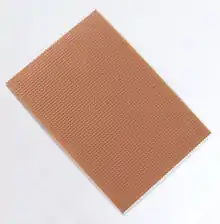
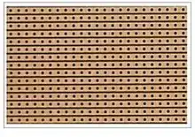 Veroboard piece | |
| Product | Electronic component |
|---|---|
| Inventor | Terry Fitzpatrick |
| Company | Vero Electronics Ltd |
| Country | UK |
| Availability | 1960 - present |
In using the board, breaks are made in the tracks, usually around holes, to divide the strips into multiple electrical nodes. With care, it is possible to break between holes to allow for components that have two pin rows only one position apart such as twin row headers for IDCs.
Stripboard is not designed for surface-mount components, though it is possible to mount many such components on the track side, particularly if tracks are cut/shaped with a knife or small cutting disc in a rotary tool.
The first single-size Veroboard product was the forerunner of the numerous types of prototype wiring board which, with worldwide use over five decades, have become known as stripboard.
The generic terms 'veroboard' and 'stripboard' are now taken to be synonymous.
History
By the mid-1950s, the printed circuit board (PCB) had become commonplace in electronics production.[1]
In early 1959, the VPE Electronics Department was formed when managing director Geoffrey Verdon-Roe hired two former Saunders-Roe Ltd employees, Peter H Winter (aircraft design department) and Terry Fitzpatrick (electronics division).
After the failure of a project to develop machine tool control equipment, the department remained operative as a result of success with the invention and development of the new material.
New equipment using PCBs was displayed at the 1959 Radio and Electronics Components Manufacturers Federation (RECMF) Exhibition held in The Dorchester Hotel, Park Lane, London.[2]
The usual configuration for most of the PCBs of that time had components placed in a regular pattern with the circuit formed by maze-like conductive pathways. An interesting alternative, proposed by Fitzpatrick after visiting the RECMF Exhibition on behalf of VPE, envisaged a standard circuit board carrying straight-line conductors on which the components could be suitably dispersed and connected to the conductors to produce the required circuit.
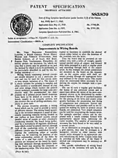
A patent application was immediately filed 25 May 1959[3] and the invention was developed for Vero by associates Winter, Fitzpatrick and machine shop engineers.
The advent of the Arduino integrated development environment, designed to introduce computer programming to newcomers unfamiliar with software development, presents a new opportunity to use Veroboard.[4] Arduino development regularly involves the use of 'shields', which plug into the main Arduino board using standard 0.1 in header connections and carry project-specific I/O hardware. However the Arduino design makes this difficult, as one of the four header sockets is offset from the 0.1 in spacing of the others by 0.05 in.
The British company Vero Technologies Ltd currently holds the UK trademark for Veroboard.[5] In the Americas the Veroboard trademark is now held by the Canadian company Pixel Print Ltd. of Vancouver.[6]
Hole spacing
Stripboard holes are drilled on 0.1 inches (2.54 mm) centers. This spacing allows components having pins with a 0.1 inches (2.54 mm) spacing to be inserted. Compatible parts include DIP ICs, sockets for ICs, some types of connectors, and other devices.
Stripboards have evolved over time into several variants and related products. For example, a larger version using a 0.15 inch (3.81 mm) grid and larger holes is available, but is generally less popular (presumably because it does not match up with standard IC pin spacing).
Board dimensions
Stripboard is available in a variety of sizes. One common size (at least in the United Kingdom) is 160 mm x 100 mm.[7]
Assemblies
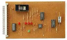
The components are usually placed on the plain side of the board, with their leads protruding through the holes. The leads are then soldered to the copper tracks on the other side of the board to make the desired connections, and any excess wire is cut off. The continuous tracks may be easily and neatly cut as desired to form breaks between conductors using a 3 mm twist drill, a hand cutter made for the purpose, or a knife. Tracks may be linked up on either side of the board using wire. With practice, very neat and reliable assemblies can be created, though such a method is labour-intensive and therefore unsuitable for production assemblies except in very small quantity.
External wire connections to the board are made either by soldering the wires through the holes or, for wires too thick to pass through the holes, by soldering them to specially made pins called Veropins which fit tightly into the holes. Alternatively, some types of connectors have a suitable pin spacing to be inserted directly into the board.
Production
Production of the proposed new product, Veroboard, was undertaken by the VPE machine tool department.
Bought-in sheets of 1.6 mm (0.06 in) copper-clad SRBP printed circuit material were cut to give 122 mm x 456 mm (4.8 in x 18 in) size boards with the individual boards then being machined to form the final product according to the original Veroboard specification. A multiple milling cutter tool, which comprised a bank of side-and-face cutters with suitably shaped cutting teeth, was fabricated, to be used in removing part of the bonded copper on each board leaving 21 conductive strips.[8]
For a second operation a special tool with 63 hardened punch bits 1.35 mm (0.052 in) in diameter mounted on a solid base block was constructed to repeat-punch a matrix of holes, on 0.2 in (5.1 mm) spacing, through the copper strips and the base board.
Many dimensional, material quality, and tooling problems were encountered before finished boards of acceptable quality could be produced in quantity. These machining problems were encountered due to the non-availability, in 1960, of advanced printed circuit board milling and drilling techniques or facilities for chemical milling (etching) the copper strips.
In 1961, as production rates improved with experience, Vero Electronics Ltd was formed as a separate company to market the increasing sales of Veroboard.
Use
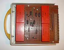
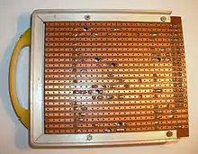
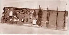
As with other stripboards, in using Veroboard, components are suitably positioned and soldered to the conductors to form the required circuit. Breaks can be made in the tracks, usually around holes, to divide the strips into multiple electrical nodes enabling increased circuit complexity.
This type of wiring board may be used for initial electronic circuit development, to construct prototypes for bench testing or in the production of complete electronic units in small quantity.
Veroboard was first used for prototype construction within Vero Electronics Department in 1961. The images of a binary decade counter sub-unit clearly show both the assembled components and the copper conductors with the required discontinuities.
A number of these sub-units were interconnected through connectors mounted on a motherboard similar to that shown in the Veroboard Display image and comprised a very early PCB-based backplane system. Each sub-unit had a digital capacity equivalent to 1/2 byte of data storage - i.e. 2,000,000 would be required to store 1 megabyte.
Two forms of Veroboard are produced with hole pitch of 2.54 mm (0.1 in) or 3.5 mm (0.15 in). The larger pitch is and was considered easier to assemble, especially at a time when many constructors were still more familiar with valves and tag strips.
The increasingly popular integrated circuits in dual in-line packages would only fit the 0.1 boards. Very soon 0.1 pitch became by far the dominant form. Integrated circuits and the common layout of short parallel strips protruding from the sides of an IC package encouraged the development of specialist boards such as Verostrip. This was a long, thin board with the copper strips arranged transversely, rather than the usual lengthwise. A ready-cut central gap was provided to isolate the sides of the IC.
A 1979 Vero Electronics Ltd production drawing shows a special Veroboard product made for RS Components Ltd.[9] The versatility of the veroboard/stripboard type of product is demonstrated by the large number of design examples currently (2013-07) to be found on the Internet.[10]
Variations
Stripboard is available from many vendors. All versions have copper strips on one side. Some are made using printed circuit board etching and drilling techniques, although some have milled strips and punched holes. The original Veroboard used FR-2 synthetic-resin-bonded paper (SRBP) (also known as phenolic board) as the base board material. Some versions of stripboard now use higher quality FR-4 (fiberglass-reinforced epoxy laminate) material.[11]
Comparison with other systems
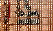
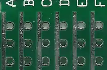
For high density prototyping, especially of digital circuits, wire wrap is faster and more reliable than Stripboard for experienced personnel.[12]
Veroboard is similar in concept and usage to a plug-in breadboard, but is cheaper and more permanent—connections are soldered and while some limited reuse may be possible, more than a few cycles of soldering and desoldering are likely to render both the components and the board unusable. In contrast, breadboard connections are held by friction, and the breadboard can be reused many times. However, a breadboard is not very suitable for prototyping that needs to remain in a set configuration for an appreciable period of time nor for physical mock-ups containing a working circuit or for any environment subject to vibration or movement.
Stripboards have further evolved into a larger class of prototype boards, available in different shapes and sizes, with different conductive trace layouts.
For example, one variant is called a TriPad board. This is similar to stripboard, except that the conductive tracks do not run continuously along the board but are broken into sections, each of which spans three holes. This allows the legs of two or three components to be easily linked together in the circuit conveniently without the need for track breaks to be made. However, in order to link more than three holes together, wire links or bridges must be formed and this can result in a less compact layout than is possible with ordinary stripboard.
Another variant is Perf+.[13] This is best described as a selective stripboard. Instead of having all the holes connected together in a strip, a Perf+ board can have holes connected to the bus using a small dab of solder. On the other side the busses run in another direction, allowing compact layouts of complicated circuits by passing signals over each other on different layers of the board.
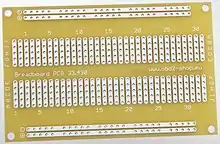
Other prototype board variants have generic layouts to simplify building prototypes with integrated circuits, typically in DIP shapes, or with transistors (pads forming triangles). In particular, some boards mimic the layout of breadboards, to simplify moving a non-permanent prototype on a breadboard to a permanent construction on a PCB. Some types of boards have patterns for connectors on the periphery, like DB9 or IDC headers, to allow connectors with non-standard pin spacings to be easily used.[14] Some come in special physical shapes, to be used to prototype plug-in boards for computer bus systems.
References
- Kearney, Georgina (19 February 2016). "The History of Printed Circuit Boards". mint-tek.com. Mint Tek Circuits. Retrieved 24 April 2020.
- The Dorchester Hotel has no existing record for 1959 events.
- London, The Patent Office (27 November 2013). "Veroboard Patent" (scan). Retrieved 24 April 2020.
- Chantrell, Nathan. "'Veroduino'".
- UK Trademark 824,961, Intellectual Property Office website
- Veroboard.com. "Pixel Print".
- Prototype and development boards from RS Components The board size with the largest number of products listed is 160 mm x 100 mm.
- "Side-and-face Mill Cutter".Google Images
- "Veroboard product for RS Components" (PDF). Archived from the original (PDF) on 2012-03-30.,Vero Electronics production drawing
- "Veroboard Design Examples".Google Images
- BusBoard Prototype Systems Ltd. "ST3U StripBoard Datasheet" Retrieved on 2010-10-20. Archived 2011-09-11 at the Wayback Machine
- Bilotta, Anthony J.: Connections in Electronic Assemblies. Marcel Dekker: 1985. ISBN 0-8247-7319-5
- Original Kickstarter for Perf+. "Perf+ the perfboard reinvented" Retrieved on 2015-4-17.
- BusBoard Prototype Systems Ltd. "PR3UC ProtoBoard With Connectors Datasheet" Retrieved on 2010-10-20.