Kikuchi lines (physics)
Kikuchi lines are patterns of electrons formed by scattering. They pair up to form bands in electron diffraction from single crystal specimens, there to serve as "roads in orientation-space" for microscopists uncertain of what they are looking at. In transmission electron microscopes, they are easily seen in diffraction from regions of the specimen thick enough for multiple scattering.[1] Unlike diffraction spots, which blink on and off as one tilts the crystal, Kikuchi bands mark orientation space with well-defined intersections (called zones or poles) as well as paths connecting one intersection to the next.
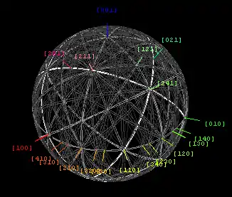
Experimental and theoretical maps of Kikuchi band geometry, as well as their direct-space analogs e.g. bend contours, electron channeling patterns, and fringe visibility maps are increasingly useful tools in electron microscopy of crystalline and nanocrystalline materials.[2] Because each Kikuchi line is associated with Bragg diffraction from one side of a single set of lattice planes, these lines can be labeled with the same Miller or reciprocal-lattice indices that are used to identify individual diffraction spots. Kikuchi band intersections, or zones, on the other hand are indexed with direct-lattice indices i.e. indices which represent integer multiples of the lattice basis vectors a, b and c.
Kikuchi lines are formed in diffraction patterns by diffusely scattered electrons, e.g. as a result of thermal atom vibrations.[3] The main features of their geometry can be deduced from a simple elastic mechanism proposed in 1928 by Seishi Kikuchi,[4] although the dynamical theory of diffuse inelastic scattering is needed to understand them quantitatively.[5]
In x-ray scattering, these lines are referred to as Kossel lines[6] (named after Walther Kossel).
Recording experimental Kikuchi patterns and maps
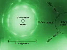
The figure at left shows the Kikuchi lines leading to a silicon [100] zone, taken with the beam direction approximately 7.9° away from the zone along the (004) Kikuchi band. The dynamic range in the image is so large that only portions of the film are not overexposed. Kikuchi lines are much easier to follow with dark-adapted eyes on a fluorescent screen, than they are to capture unmoving on paper or film, even though eyes and photographic media both have a roughly logarithmic response to illumination intensity. Fully quantitative work on such diffraction features is therefore assisted by the large linear dynamic range of CCD detectors.[7]
This image subtends an angular range of over 10° and required use of a shorter than usual camera length L. The Kikuchi band widths themselves (roughly λL/d where λ/d is approximately twice the Bragg angle for the corresponding plane) are well under 1°, because the wavelength λ of electrons (about 1.97 picometres in this case) is much less than the lattice plane d-spacing itself. For comparison, the d-spacing for silicon (022) is about 192 picometres while the d-spacing for silicon (004) is about 136 picometres.
The image was taken from a region of the crystal which is thicker than the inelastic mean free path (about 200 nanometres), so that diffuse scattering features (the Kikuchi lines) would be strong in comparison to coherent scattering features (diffraction spots). The fact that surviving diffraction spots appear as disks intersected by bright Kikuchi lines means that the diffraction pattern was taken with a convergent electron beam. In practice, Kikuchi lines are easily seen in thick regions of either selected area or convergent beam electron diffraction patterns, but difficult to see in diffraction from crystals much less than 100 nm in size (where lattice-fringe visibility effects become important instead). This image was recorded in convergent beam, because that too reduces the range of contrasts that have to be recorded on film.
Compiling Kikuchi maps which cover more than a steradian requires that one take many images at tilts changed only incrementally (e.g. by 2° in each direction). This can be tedious work, but may be useful when investigating a crystal with unknown structure as it can clearly unveil the lattice symmetry in three dimensions.[8]
Kikuchi line maps and their stereographic projection
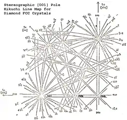
The figure at left plots Kikuchi lines for a larger section of silicon's orientation space. The angle subtended between the large [011] and [001] zones at the bottom is 45° for silicon. Note that four-fold zone in the lower right (here labeled [001]) has the same symmetry and orientation as the zone labeled [100] in the experimental pattern above, although that experimental pattern only subtends about 10°.
Note also that the figure at left is excerpted from a stereographic projection centered on that [001] zone. Such conformal projections allow one to map pieces of spherical surface onto a plane while preserving the local angles of intersection, and hence zone symmetries. Plotting such maps requires that one be able to draw arcs of circles with a very large radius of curvature. The figure at left, for example, was drawn before the advent of computers and hence required the use of a beam compass. Finding a beam compass today might be fairly difficult, since it is much easier to draw curves having a large radius of curvature (in two or three dimensions) with help from a computer.
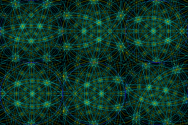
The angle-preserving effect of stereographic plots is even more obvious in the figure at right, which subtends a full 180° of the orientation space of a face-centered or cubic close packed crystal e.g. like that of Gold or Aluminum. The animation follows {220} fringe-visibility bands of that face-centered cubic crystal between <111> zones, at which point rotation by 60° sets up travel to the next <111> zone via a repeat of the original sequence. Fringe-visibility bands have the same global geometry as do Kikuchi bands, but for thin specimens their width is proportional (rather than inversely proportional) to d-spacing. Although the angular field width (and tilt range) obtainable experimentally with Kikuchi bands is generally much smaller, the animation offers a wide-angle view of how Kikuchi bands help informed crystallographers find their way between landmarks in the orientation space of a single crystal specimen.
Real space analogs
Kikuchi lines serve to highlight the edge on lattice planes in diffraction images of thicker specimens. Because Bragg angles in the diffraction of high energy electrons are very small (~1⁄4 degrees for 300 keV), Kikuchi bands are quite narrow in reciprocal space. This also means that in real space images, lattice planes edge-on are decorated not by diffuse scattering features but by contrast associated with coherent scattering. These coherent scattering features include added diffraction (responsible for bend contours in curved foils), more electron penetration (which gives rise to electron channeling patterns in scanning electron images of crystal surfaces), and lattice fringe contrast (which results in a dependence of lattice fringe intensity on beam orientation which is linked to specimen thickness). Although the contrast details differ, the lattice plane trace geometry of these features and of Kikuchi maps are the same.
Bend contours and rocking curves
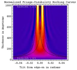
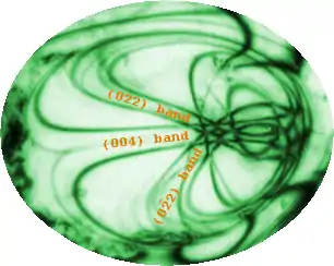
Rocking curves[9] (left) are plots of scattered electron intensity, as a function of the angle between an incident electron beam and the normal to a set of lattice planes in the specimen. As this angle changes in either direction from edge-on (at which orientation the electron beam runs parallel to the lattice planes and perpendicular to their normal), the beam moves into Bragg diffracting condition and more electrons are diffracted outside the microscope's back focal plane aperture, giving rise to the dark-line pairs (bands) seen in the image of the bent silicon foil shown in the image at right.
The [100] bend contour "spider" of this image, trapped in a region of silicon that was shaped like an oval watchglass less than a micrometre in size, was imaged with 300 keV electrons. If you tilt the crystal, the spider moves toward the edges of the oval as though it is trying to get out. For example, in this image the spider's [100] intersection has moved to the right side of the ellipse as the specimen was tilted to the left.
The spider's legs, and their intersections, can be indexed as shown in precisely the same way as the Kikuchi pattern near [100] in the section on experimental Kikuchi patterns above. In principle, one could therefore use this bend contour to model the foil's vector tilt (with milliradian accuracy) at all points across the oval.
Lattice fringe visibility maps
As you can see from the rocking curve above, as specimen thickness moves into the 10 nanometre and smaller range (e.g. for 300 keV electrons and lattice spacings near 0.23 nm) the angular range of tilts that give rise to diffraction and/or lattice-fringe contrast becomes inversely proportional to specimen thickness. The geometry of lattice-fringe visibility therefore becomes useful in the electron microscope study of nanomaterials,[10][11] just as bend contours and Kikuchi lines are useful in the study of single crystal specimens (e.g. metals and semiconductor specimens with thickness in the tenth-micrometre range). Applications to nanostructure for example include: (i) determining the 3D lattice parameters of individual nanoparticles from images taken at different tilts,[12] (ii) fringe fingerprinting of randomly oriented nanoparticle collections, (iii) particle thickness maps based on fringe contrast changes under tilt, (iv) detection of icosahedral twinning from the lattice image of a randomly oriented nanoparticle, and (v) analysis of orientation relationships between nanoparticles and a cylindrical support.
Electron channeling patterns
The above techniques all involve detection of electrons which have passed through a thin specimen, usually in a transmission electron microscope. Scanning electron microscopes, on the other hand, typically look at electrons "kicked up" when one rasters a focussed electron beam across a thick specimen. Electron channeling patterns are contrast effects associated with edge-on lattice planes that show up in scanning electron microscope secondary and/or backscattered electron images.
The contrast effects are to first order similar to those of bend contours, i.e. electrons which enter a crystalline surface under diffracting conditions tend to channel (penetrate deeper into the specimen without losing energy) and thus kick up fewer electrons near the entry surface for detection. Hence bands form, depending on beam/lattice orientation, with the now-familiar Kikuchi line geometry.
The first scanning electron microscope (SEM) image was an image of electron channeling contrast in silicon steel.[13] However, practical uses for the technique are limited because only a thin layer of abrasion damage or amorphous coating is generally adequate to obscure the contrast.[14] If the specimen had to be given a conductive coating before examination to prevent charging, this too could obscure the contrast. On cleaved surfaces, and surfaces self-assembled on the atomic scale, electron channeling patterns are likely to see growing application with modern microscopes in the years ahead.
References
- David B. Williams; C. Barry Carter (1996). Transmission electron microscopy: A textbook for materials science. Plenum Press, NY. ISBN 978-0-306-45324-3.
- K. Saruwatari; J. Akai; Y. Fukumori; N. Ozaki; H. Nagasawa; T. Kogure (2008). "Crystal orientation analyses of biominerals using Kikuchi patterns in TEM". J. Mineral. Petrol. Sci. 103: 16–22. doi:10.2465/jmps.070611.
- Earl J. Kirkland (1998). Advanced computing in electron microscopy. Plenum Press, NY. p. 151. ISBN 978-0-306-45936-8.
- S. Kikuchi (1928). "Diffraction of Cathode Rays by Mica". Japanese Journal of Physics. 5 (3061): 83–96. Bibcode:1928Natur.121.1019N. doi:10.1038/1211019a0.
- P. Hirsch; A. Howie; R. Nicholson; D. W. Pashley; M. J. Whelan (1977). Electron microscopy of thin crystals. Butterworths/Krieger, London/Malabar FL. ISBN 978-0-88275-376-8.
- R. W. James (1982). "Chapter VIII". The Optical Principles of the Diffraction of X-Rays'. Ox Bow Press, Woodbridge, Connecticut. ISBN 978-0-918024-23-7.
- J. C. H. Spence and J. Zuo (1992). "Ch. 9". Electron microdiffraction. Plenum, New York. ISBN 978-0-306-44262-9.
- E. Levine; W. L. Bell; G. Thomas (1966). "Further applications of Kikuchi diffraction patterns; Kikuchi maps". Journal of Applied Physics. 37 (5): 2141–2148. Bibcode:1966JAP....37.2141L. doi:10.1063/1.1708749.
- H. Hashimoto; A. Howie; M. J. Whelan (1962). "Anomalous Electron Absorption Effects in Metal Foils: Theory and Comparison with Experiment". Proceedings of the Royal Society A. 269 (1336): 80. Bibcode:1962RSPSA.269...80H. doi:10.1098/rspa.1962.0164. S2CID 97942498.
- P. Fraundorf; Wentao Qin; P. Moeck; Eric Mandell (2005). "Making sense of nanocrystal lattice fringes". Journal of Applied Physics. 98 (11): 114308–114308–10. arXiv:cond-mat/0212281. Bibcode:2005JAP....98k4308F. doi:10.1063/1.2135414. S2CID 13681236.
- P. Wang; A. L. Bleloch; U. Falke; P. J. Goodhew (2006). "Geometric aspects of lattice contrast visibility in nanocrystalline materials using HAADF STEM". Ultramicroscopy. 106 (4–5): 277–283. doi:10.1016/j.ultramic.2005.09.005.
- Wentao Qin; P. Fraundorf (2003). "Lattice parameters from direct-space images at two tilts". Ultramicroscopy. 94 (3–4): 245–262. arXiv:cond-mat/0001139. doi:10.1016/S0304-3991(02)00335-2. PMID 12524195. S2CID 10524417.
- Knoll M. (1935). "Aufladepotentiel und sekundäremission elektronenbestrahlter körper (Static potential and secondary emission of bodies under electron irradiation)". Z. Tech. Phys. 11: 467–475.
- J. I. Goldstein; D. E. Newbury; P. Echlin; D. C. Joy; A. D. Romig Jr.; C. E. Lyman; C. Fiori; E. Lifshin (1992). Scanning electron microscopy and X-ray microanalysis. Plenum Press, NY. ISBN 978-0-306-44175-2.
External links
- Calculate patterns with WebEMApS at UIUC.
- Some interactive 3D maps at UM Saint Louis.
- Calculate Kikuchi map or patterns with free software PTCLab .