Indium antimonide
Indium antimonide (InSb) is a crystalline compound made from the elements indium (In) and antimony (Sb). It is a narrow-gap semiconductor material from the III-V group used in infrared detectors, including thermal imaging cameras, FLIR systems, infrared homing missile guidance systems, and in infrared astronomy. Indium antimonide detectors are sensitive to infrared wavelengths between 1 and 5 μm.
 | |
 | |
| Identifiers | |
|---|---|
3D model (JSmol) |
|
| ChemSpider | |
| ECHA InfoCard | 100.013.812 |
| EC Number |
|
PubChem CID |
|
| RTECS number |
|
| UNII | |
| UN number | 1549 |
CompTox Dashboard (EPA) |
|
| |
| |
| Properties | |
| InSb | |
| Molar mass | 236.578 g·mol−1 |
| Appearance | Dark grey, metallic crystals |
| Density | 5.7747 g⋅cm−3[1] |
| Melting point | 524 °C (975 °F; 797 K)[1] |
| Band gap | 0.17 eV |
| Electron mobility | 7.7 mC⋅s⋅g−1 (at 27 °C) |
| Thermal conductivity | 180 mW⋅K−1⋅cm−1 (at 27 °C) |
Refractive index (nD) |
4[2] |
| Structure | |
| Zincblende | |
| T2d-F-43m | |
a = 0.648 nm | |
| Tetrahedral | |
| Thermochemistry[3] | |
Heat capacity (C) |
49.5 J·K−1·mol−1 |
Std molar entropy (S⦵298) |
86.2 J·K−1·mol−1 |
Std enthalpy of formation (ΔfH⦵298) |
−30.5 kJ·mol−1 |
Gibbs free energy (ΔfG⦵) |
−25.5 kJ·mol−1 |
| Hazards | |
| GHS labelling: | |
  [4] [4] | |
| Warning | |
| H302, H332, H411 | |
| P273 | |
| Safety data sheet (SDS) | External SDS |
| Related compounds | |
Other anions |
Indium nitride Indium phosphide Indium arsenide |
Except where otherwise noted, data are given for materials in their standard state (at 25 °C [77 °F], 100 kPa).
Infobox references | |
Indium antimonide was a very common detector in the old, single-detector mechanically scanned thermal imaging systems. Another application is as a terahertz radiation source as it is a strong photo-Dember emitter.
History
The intermetallic compound was first reported by Liu and Peretti in 1951, who gave its homogeneity range, structure type, and lattice constant.[5] Polycrystalline ingots of InSb were prepared by Heinrich Welker in 1952, although they were not very pure by today's semiconductor standards. Welker was interested in systematically studying the semiconducting properties of the III-V compounds. He noted how InSb appeared to have a small direct band gap and a very high electron mobility.[6] InSb crystals have been grown by slow cooling from liquid melt at least since 1954.[7]
Physical properties
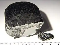
InSb has the appearance of dark-grey silvery metal pieces or powder with vitreous lustre. When subjected to temperatures over 500 °C, it melts and decomposes, liberating antimony and antimony oxide vapors.
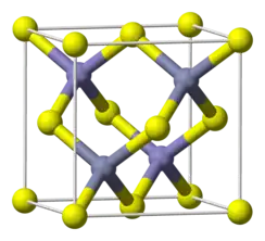
The crystal structure is zincblende with a 0.648 nm lattice constant.[8]
Electronic properties

InSb is a narrow direct band gap semiconductor with an energy band gap of 0.17 eV at 300 K and 0.23 eV at 80 K.[8]
Undoped InSb possesses the largest ambient-temperature electron mobility of 78000 cm2/(V⋅s),[9] electron drift velocity, and ballistic length (up to 0.7 μm at 300 K)[8] of any known semiconductor, except for carbon nanotubes.
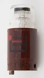
Indium antimonide photodiode detectors are photovoltaic, generating electric current when subjected to infrared radiation. InSb's internal quantum efficiency is effectively 100% but is a function of the thickness particularly for near bandedge photons.[10] Like all narrow bandgap materials InSb detectors require periodic recalibrations, increasing the complexity of the imaging system. This added complexity is worthwhile where extreme sensitivity is required, e.g. in long-range military thermal imaging systems. InSb detectors also require cooling, as they have to operate at cryogenic temperatures (typically 80 K). Large arrays (up to 2048×2048 pixels) are available.[11] HgCdTe and PtSi are materials with similar use.
A layer of indium antimonide sandwiched between layers of aluminium indium antimonide can act as a quantum well. In such a heterostructure InSb/AlInSb has recently been shown to exhibit a robust quantum Hall effect.[12] This approach is studied in order to construct very fast transistors.[13] Bipolar transistors operating at frequencies up to 85 GHz were constructed from indium antimonide in the late 1990s; field-effect transistors operating at over 200 GHz have been reported more recently (Intel/QinetiQ). Some models suggest that terahertz frequencies are achievable with this material. Indium antimonide semiconductor devices are also capable of operating with voltages under 0.5 V, reducing their power requirements.
Growth methods
InSb can be grown by solidifying a melt from the liquid state (Czochralski process), or epitaxially by liquid phase epitaxy, hot wall epitaxy or molecular beam epitaxy. It can also be grown from organometallic compounds by MOVPE.
Device applications
- Thermal image detectors using photodiodes or photoelectromagnetic detectors
- Magnetic field sensors using magnetoresistance or the Hall effect
- Fast transistors (in terms of dynamic switching). This is due to the high carrier mobility of InSb.
- In some of the detectors of the Infrared Array Camera on the Spitzer Space Telescope
References
- Haynes, p. 4.66
- Haynes, pp. 12.156
- Haynes, pp. 5.22
- "Indium Antimonde". American Elements. Retrieved June 20, 2019.
- Liu, T.S.; Peretti, E.A. (1951). "The Lattice Parameter of InSb". Trans AIME. 191: 791.
- Orton, J.W. (2009). Semiconductors and the Information Revolution: Magic Crystals that Made IT Happen. Academic Press. pp. 138–9. ISBN 9780444532404.
- Avery, D G; Goodwin, D W; Lawson, W D; Moss, T S (1954). "Optical and Photo-Electrical Properties of Indium Antimonide". Proceedings of the Physical Society. Series B. 67 (10): 761. Bibcode:1954PPSB...67..761A. doi:10.1088/0370-1301/67/10/304.
- Properties of Indium Antimonide (InSb). ioffe.ru
- Rode, D. L. (1971). "Electron Transport in InSb, InAs, and InP". Physical Review B. 3 (10): 3287–3299. Bibcode:1971PhRvB...3.3287R. doi:10.1103/PhysRevB.3.3287.
- Avery, D G; Goodwin, D W; Rennie, Miss A E (1957). "New infra-red detectors using indium antimonide". Journal of Scientific Instruments. 34 (10): 394. Bibcode:1957JScI...34..394A. doi:10.1088/0950-7671/34/10/305.
- Beckett, M.G. (1995). "3. Camera". High Resolution Infrared Imaging (PhD). Cambridge University. uk.bl.ethos.388828.
- Alexander-Webber, J. A.; Baker, A. M. R.; Buckle, P. D.; Ashley, T.; Nicholas, R. J. (2012-07-05). "High-current breakdown of the quantum Hall effect and electron heating in InSb/AlInSb". Physical Review B. American Physical Society (APS). 86 (4): 045404. Bibcode:2012PhRvB..86d5404A. doi:10.1103/physrevb.86.045404.
- Will Knight (2005-02-10). "'Quantum well' transistor promises lean computing". New Scientist. Retrieved 2020-01-11.
Cited sources
- Haynes, William M., ed. (2016). CRC Handbook of Chemistry and Physics (97th ed.). CRC Press. ISBN 9781498754293.