Carrier scattering
Defect types include atom vacancies, adatoms, steps, and kinks that occur most frequently at surfaces due to the finite material size causing crystal discontinuity. What all types of defects have in common, whether surface or bulk defects, is that they produce dangling bonds that have specific electron energy levels different from those of the bulk. This difference occurs because these states cannot be described with periodic Bloch waves due to the change in electron potential energy caused by the missing ion cores just outside the surface. Hence, these are localized states that require separate solutions to the Schrödinger equation so that electron energies can be properly described. The break in periodicity results in a decrease in conductivity due to defect scattering.
Electronic energy levels of semiconductor dangling bonds

A simpler and more qualitative way of determining dangling bond energy levels is with Harrison diagrams.[1][2] Metals have non-directional bonding and a small Debye length which, due to their charged nature, makes dangling bonds inconsequential if they can even be considered to exist. Semiconductors are dielectrics so electrons can feel and become trapped at defect energy states. The energy levels of these states are determined by the atoms that make up the solid. Figure 1 shows the Harisson diagram for the elemental semiconductor Si. From left to right, s-orbital and p-orbital hybridization promotes sp3 bonding which, when multiple sp3 Si-Si dimers are combined to form a solid, defines the conduction and valence bands. If a vacancy were to exist, such as those on each atom at the solid/vacuum interface, it would result in at least one broken sp3 bond which has an energy equal to that of single self hybridized Si atoms as shown in Figure 1. This energy corresponds to roughly the middle of the bandgap of Si, ~0.55eV above the valence band. Certainly this is the most ideal case whereas the situation would be different if bond passivation (see below) and surface reconstruction, for example, were to occur. Experimentally, the energies of these states can be determined using absorption spectroscopy or X-ray photoelectron spectroscopy, for example, if instrument sensitivity and/or defect density are high enough.

Compound semiconductors, such as GaAs, have dangling bond states that are nearer to the band edges (see Figure 2). As bonding becomes increasingly more ionic, these states can even act as dopants. This is the cause of the well known difficulty of GaN p-type doping where N vacancies are abundant due to its high vapor pressure resulting in high Ga dangling bond density. These states are close to the conduction band edge and therefore act as donors. When p-type acceptor dopants are introduced, they are immediately compensated for by the N vacancies. With these shallow states, their treatment is often considered as an analogue to the hydrogen atom as follows for the case of either anion or cation vacancies (hole effective mass, m*, for cation and electron m* for anion vacancies). The binding energy, Ec-Edb, is
where U=-q2/(4πεεrr) is the electrostatic potential between an electron occupying the dangling bond and its ion core with ε, the free space permittivity constant, εr, the relative permittivity, and r the electron-ion core separation. The simplification that the electron translational energy, KE=-U/2, is due to the virial theorem for centrosymmetric potentials. As described by the Bohr model, r is subject to quantization
.
The electron momentum is p=mv=h/λ such that
resulting in
and
.
This treatment loses accuracy as the defects tend away from either band edge.
Defect scattering
The dangling bond energy levels are eigenvalues of wavefunctions that describe electrons in the vicinity of the defects. In the typical consideration of carrier scattering, this corresponds to the final state in Fermi's golden rule of scattering frequency:
with H' being the interaction parameter and the Dirac delta function, δ(Ef-Ei), indicating elastic scattering. The simple relation 1/τ= Σk',k Sk'k makes this a useful equation for characterizing material transport properties when used in conjunction with σ = ne2τ /m* and Matthiessen's rule to incorporate other scattering processes.
The value of Sk'k is primarily determined by the interaction parameter, H'. This term is different depending on whether shallow or deep states are considered. For shallow states, H' is the perturbation term of the redefined Hamiltonian H=Ho+H', with Ho having an eigenvalue energy of Ei. The matrix for this case is [3]
where k' is the final state wavevector of which there is only one value since the defect density is small enough to not form bands (~<1010/cm2). Using the Poisson equation for Fourier periodic point charges,
,
gives the Fourier coefficient of the potential from a dangling bond Vq=e/(q2εεrV) where V is volume. This results in
where qs is the Debye length wavevector correction due to charge screening. Then, the scattering frequency is
where n is the volumetric defect density. Performing the integration, utilizing |k|=|k'|, gives
.
The above treatment falters when the defects are not periodic since dangling bond potentials are represented with a Fourier series. Simplifying the sum by the factor of n in Eq (10) was only possible due to low defect density. If every atom (or possibly every other) were to have one dangling bond, which is quite reasonable for a non-reconstructed surface, the integral on k' must also be performed. Due to the use of perturbation theory in defining the interaction matrix, the above assumes small values of H' or, shallow defect states close to band edges. Fortunately, Fermi's golden rule itself is quite general and can be used for deep state defects if the interaction between conduction electron and defect is understood well enough to model their interaction into an operator that replaces H'.
Experimental measurements

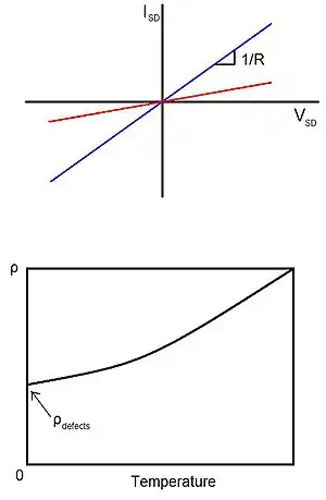
Determination of the extent these dangling bonds have on electrical transport can be experimentally observed fairly readily. By sweeping the voltage across a conductor (Figure 3), the resistance, and with a defined geometry, the conductivity of the sample can be determined. As mentioned before, σ = ne2τ /m*, where τ can be determined knowing n and m* from the Fermi level position and material band structure. Unfortunately, this value contains effects from other scattering mechanisms such as due to phonons. This gains usefulness when the measurement is used alongside Eq (11) where the slope of a plot of 1/τ versus n makes Ec-Edb calculable and the intercept determines 1/τ from all but defect scattering processes. This requires the assumption that phonon scattering (among other, possibly negligible processes) is independent of defect concentration.
In a similar experiment, one can just lower the temperature of the conductor (Figure 3) so that phonon density decreases to negligible allowing defect dominant resistivity. With this case, σ = ne2τ /m* can be used to directly calculate τ for defect scattering.
Passivation

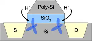
Surface defects can always be "passivated" with atoms to purposefully occupy the corresponding energy levels so that conduction electrons cannot scatter into these states (effectively decreasing n in Eq (10)). For example, Si passivation at the channel/oxide interface of a MOSFET with hydrogen (Figure 4) is a typical procedure to help reduce the ~1010 cm−2 defect density by up to a factor of 12[4] thereby improving mobility and, hence, switching speeds. Removal of intermediary states which would otherwise reduce tunneling barriers also decreases gate leakage current and increases gate capacitance as well as transient response. The effect is that the Si sp3 bonding becomes fully satisfied. The obvious requirement here is the ability for the semiconductor to oxidize the passivating atom or, Ec-Edb + χ > EI, with the semiconductor electron affinity χ and atom ionization energy EI.
Phonon scattering
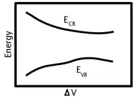
We now consider carrier scattering with lattice deformations termed phonons. Consider the volumetric displacement such a propagating wave produces, , which consequently results in a time-dependent strain, where a simple plane wave is used to describe the phonon propagation, . Displacement of atoms away from their equilibrium positions generally causes a change in the electronic band structure (Figure 5) where, for scattering, we are concerned with electrons in the conduction band with energy ~ECB,
.
The empirical parameter, ZDP, is termed the deformation potential and describes electron-phonon coupling strength. Multiplying by the phonon population (Bose–Einstein distribution, Nq) gives the total deformation potential,

(the reason for the root will be apparent below). Here, the + corresponds to phonon emission and – for phonon absorption during the scattering event. A note, because for transverse phonons, only interactions with longitudinal phonons are non-zero. Therefore, the complete interaction matrix is
where the Kronecker delta enforces momentum conservation and arises from assuming the electronic wavefunctions (final state, , and initial state, ) are plane waves as well.
Acoustic phonons
Using Fermi's golden rule, the scattering rate for low energy acoustic phonons can be approximated. The interaction matrix for these phonons is
with the phonon angular frequency ωq=cq, volume V, solid density ρ, and phonon group velocity c.[5] Plugging this into Eq. 6 gives
.
With the assumptions that Nq>>1, ħω<<kT and g(E') ~ g(E) (which generally holds for 3D crystals since conduction electron energies are generally much greater than ħω and g(E) lacks any van Hove singularity) gives the scattering rate:
where g(E) is the electronic density of states for which the 3-dimensional solution with parabolic dispersion was used to obtain the final answer.
Optical phonons
Typically, phonons in the optical branches of vibrational dispersion relationships have energies on the order of or greater than kT and, therefore, the approximations ħω<<kT and Nq>>1 cannot be made. Yet, a reasonable route that still provides a detour from dealing with complex phonon dispersions is using the Einstein model which states that only one phonon mode exists in solids. For optical phonons, this approximation turns out to be sufficient due to very little slope variation in ω(q) and, thus, we can claim ħω(q) ≅ ħω, a constant. Consequently, Nq is also a constant (only T dependent). The last approximation, g(E')=g(E±ħω) ~ g(E), cannot be made since ħω ~ E and there is no workaround for it, but the added complexity to the sum for τ is minimal.
.
The sum turns to the density of states at E' and the Bose–Einstein distribution can be taken out of the sum due to ħω(q) ≅ ħω.
Notes
- Harrison, Walter A., Electronic Structure and the Properties of Solids: The Physics of the Chemical Bond. San Francisco: Freeman, 1980.
- Rockett, Angus, The Materials Science of Semiconductors. New York: Springer, 2007
- Hess, Karl, Advanced Theory of Semiconductor Devices. New York: Wiley Interscience, 2000.
- Faughnan, B.; Ipri, A. C. IEEE Trans. Elec. Dev. 36, 101, 1999.
- Conwell, E. M., "High Field Transport in Semiconductors," in Solid State Physics, ed. F. Seitz, D. Turnbull, and H. Ehrenreich, Supplement 9. New York: Academic Press, 1967, p. 108.