Transmission Electron Aberration-Corrected Microscope
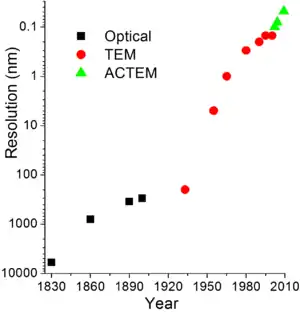
Transmission Electron Aberration-Corrected Microscope (TEAM) is a collaborative research project between four US laboratories and two companies. The project's main activity is design and application of a transmission electron microscope (TEM) with a spatial resolution below 0.05 nanometers, which is roughly half the size of an atom of hydrogen.[2]

The project is based at the Lawrence Berkeley National Laboratory in Berkeley, California and involves Argonne National Laboratory, Oak Ridge National Laboratory and Frederick Seitz Materials Research Laboratory at the University of Illinois at Urbana-Champaign, as well as FEI and CEOS companies, and is supported by the U.S. Department of Energy. The project was started in 2004; the operational microscope was built in 2008 and achieved the 0.05 nm resolution target in 2009. The microscope is a shared facility available to external users.[3]
Scientific background
It has long been known that the best achievable spatial resolution of an optical microscope, that is the smallest feature it can observe, is of the order of the wavelength of the light λ, which is about 550 nm for green light. One route to improve this resolution is to use particles with smaller λ, such as high-energy electrons. Practical limitations set a convenient electron energy to 100–300 keV that corresponds to λ = 3.7–2.0 pm. The resolution of electron microscopes is limited not by the electron wavelength, but by intrinsic imperfections of electron lenses. These are referred to as spherical and chromatic aberrations because of their similarity to aberrations in optical lenses. Those aberrations are reduced by installing in a microscope a set of specially designed auxiliary "lenses" which are called aberration correctors.[4][5]
Hardware
The TEAM is based on a commercial FEI Titan 80–300 electron microscope, which can be operated at voltages between 80 and 300 keV, both in TEM and scanning transmission electron microscopy (STEM) modes. To minimize the mechanical vibrations, the microscope is located in a separate room within a sound-proof enclosure and is operated remotely. The electron source is a Schottky type field emission gun with a relatively low energy spread of 0.8 eV at 300 keV. In order to reduce chromatic aberrations, this spread is further lowered to 0.13 eV at 300 keV and 0.08 eV at 80 kV using a Wien-filter type monochromator.[4] Both the illumination lens, which is located above the sample and is conventionally called the condenser lens, and the collection lens (called the objective lens) are equipped with fifth-order spherical aberration correctors. The electrons are further energy filtered by a GIF filter and detected by a CCD camera. The filter makes it possible to select electrons scattered by specific chemical elements and so identify individual atoms in the sample being studied.[6]
Applications
The TEAM has been tested on various crystalline solids, resolving individual atoms in GaN ([211] orientation), germanium ([114]), gold ([111]) and others, and reaching the spatial resolution below 0.05 nm (about 0.045 nm). In the images of graphene—a single sheet of graphite—not only the atoms, but also the chemical bonds could be observed. A movie has been recorded inside the microscope showing hopping of individual carbon atoms around a hole punched in a graphene sheet.[2][7][8][9] Similar pictures, resolving carbon atoms and bonds between them, have been independently produced for pentacene—a planar organic molecule consisting of five carbon rings—using a very different microscopy technique, atomic force microscopy (AFM).[10][11] In AFM, the atoms are probed not by electrons, but by a sharp vibrating tip.
References
- Pennycook, S.J.; Varela, M.; Hetherington, C.J.D.; Kirkland, A.I. (2011). "Materials Advances through Aberration-Corrected Electron Microscopy" (PDF). MRS Bulletin. 31: 36–43. doi:10.1557/mrs2006.4. S2CID 41889433.
- "Berkeley Scientists Produce First Live Action Movie of Individual Carbon Atoms in Action". March 26, 2009.
- "The TEM project timeline". lbl.gov.
- H. H. Rose (2008). "Optics of high-performance electron Microscopes". Science and Technology of Advanced Materials. 9 (1): 014107. Bibcode:2008STAdM...9a4107R. doi:10.1088/0031-8949/9/1/014107. PMC 5099802. PMID 27877933.
- N. Tanaka (2008). "Present status and future prospects of spherical aberration corrected TEM/STEM for study of nanomaterials". Sci. Technol. Adv. Mater. 9 (1): 014111. Bibcode:2008STAdM...9a4111T. doi:10.1088/1468-6996/9/1/014111. PMC 5099806. PMID 27877937.
- C. Kisielowski; et al. (2008). "Detection of Single Atoms and Buried Defects in Three Dimensions by Aberration-Corrected Electron Microscope with 0.5-Å Information Limit" (PDF). Microscopy and Microanalysis. 14 (5): 469–477. Bibcode:2008MiMic..14..469K. doi:10.1017/S1431927608080902. PMID 18793491. S2CID 12689183.
- R. Erni; et al. (2009). "Atomic-Resolution Imaging with a Sub-50-pm Electron Probe" (PDF). Physical Review Letters (Submitted manuscript). 102 (9): 096101. Bibcode:2009PhRvL.102i6101E. doi:10.1103/PhysRevLett.102.096101. PMID 19392535.
- C. O. Girit; et al. (27 March 2009). "Graphene at the Edge: Stability and Dynamics". Science. 323 (5922): 1705–8. Bibcode:2009Sci...323.1705G. doi:10.1126/science.1166999. PMID 19325110. S2CID 24762146.
- J. C. Meyer; et al. (2008). "Direct Imaging of Lattice Atoms and Topological Defects in Graphene Membranes". Nano Lett. 8 (11): 3582–6. Bibcode:2008NanoL...8.3582M. doi:10.1021/nl801386m. PMID 18563938.
- Palmer, Jason (2009-08-28). "Single molecule's stunning image". BBC News. Retrieved 2009-08-28.
- L. Gross; Mohn, F; Moll, N; Liljeroth, P; Meyer, G (2009). "The Chemical Structure of a Molecule Resolved by Atomic Force Microscopy". Science. 325 (5944): 1110–4. Bibcode:2009Sci...325.1110G. doi:10.1126/science.1176210. PMID 19713523. S2CID 9346745.