< Practical Electronics < IC
| 4049 | |||||||||||||||||||||
|---|---|---|---|---|---|---|---|---|---|---|---|---|---|---|---|---|---|---|---|---|---|
| IC Family | CMOS | ||||||||||||||||||||
| Function Family | Logic | ||||||||||||||||||||
| Description | Hex 1-Input NOT Gate | ||||||||||||||||||||
| Pins | 16 | ||||||||||||||||||||
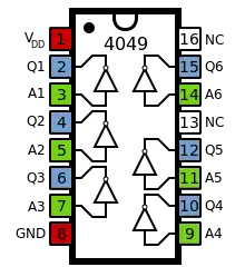
| Pinout | |||||||||||||||||||||
 | |||||||||||||||||||||
| Functional Diagram | |||||||||||||||||||||
 | |||||||||||||||||||||
| Basic TTL Counterpart | 7400 | ||||||||||||||||||||
| Truth Table (One Gate) | |||||||||||||||||||||
| |||||||||||||||||||||
The 4049 is a member of the 4000 Series CMOS range, and contains six independent NOT gates, each with two inputs. The pinout diagram, given on the right, is the standard two-input CMOS logic gate IC layout:
- Pin 1 is the positive power supply
- Pin 8 is the ground
- Pins 3, 5, 7, 9, 11 and 14 are gate inputs
- Pins 2, 4, 6, 10, 12, 14 and 15 are gate outputs
This article is issued from Wikibooks. The text is licensed under Creative Commons - Attribution - Sharealike. Additional terms may apply for the media files.